~
If:::(f(g)(Id!!)(fj) _
____
--'D'C-'-'75'-'PO~W!"E":'R~A""M":P,o,L1F':"=cER~
___
_
______
~A!OEV~.
0
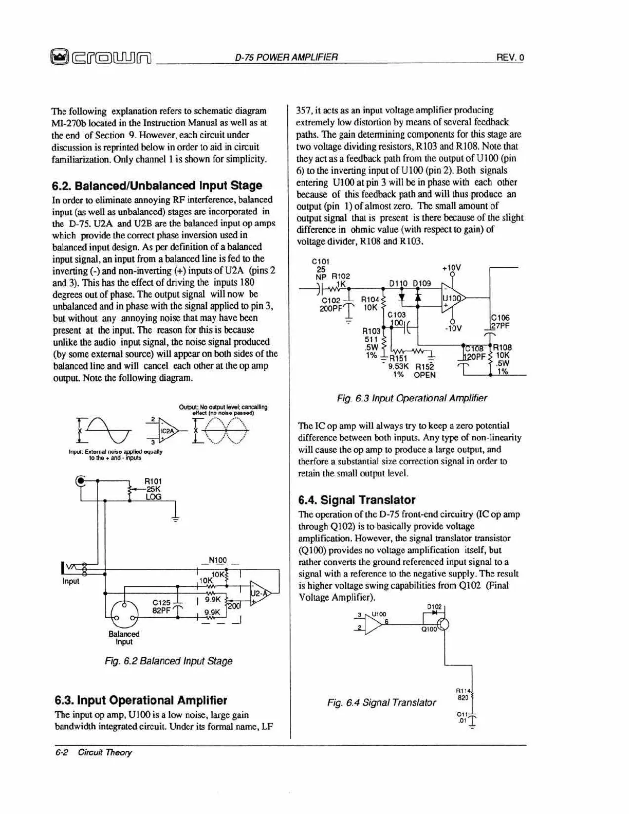
The
following
ex
planation refers
10
schematic
diagram
MI-270b
located
in
th
e
In
struction
Manual
as
well
as
al
theend
of
Section
9.
How
ever, each circuil
under
discussion
is
reprinted
below
in
order to aid
in
circu
it
familiarization. Only channell is shown
for
sim
pli
city.
6.2. Balanced/Unbalanced Input Stage
In
order
to
eliminate
annoying
RF
interference, balanced
inp
ut
(as
well
as unbalanced) s
ta
ges
ate
iocorporalCd
in
the 0-75. U2A
and
U2B
are
the
balanced input op amps
which provide
the
correct phase
inv
ersion used
in
balanced input design.
As
per definition of a balanced
input
s
ignaJ
,
an
input
from
a balanced
lin
e is
fed
10
the
inverting
(-)
and non-inverting (+) inputs
of
U2A
(pins 2
and
3). This
has
the
effect of driving the inputs J
80
degrees out
of
phase.
1be
output signal
will
now
be
unbalanced
and in phase
with
the
signal
applied
10
pin
3,
but without any annoying noise
lIlal
may
ha
ve
been
present at
the
input.
Th
e reason
for
this
is
because
unlik
e
the
aud
io input signal,
the
noise signal produced
(by
so
me
c:\temal source)
will
appear
on
both s
id
es oflhe
balanced line and
will
cancel each other at
the
op
amp
output Note
the
fo
ll
ow
ing
diagram.
IDa
''''''''
Balanced
"',,"'
el2S
82PF
I 9.9K
9.9K
Fig.
6.2 Balanced Input Stage
6.3.
Input
Operational Amplilier
The input op amp,
UlOO
is
a
low
noise. large
ga
in
bandwidlh integrated circuit.
Unde
r
its
formal
name,
LF
6-2
Circuit
Theory
357, it acts
as
an
input voltage amplifier producing
emcme1y
low
distortion
by
means
of
several feedback
paths. The
gai
n dctcrmining components
for
this
stage arc
two
voltagc dividing resistors, RI03 and
RIOS.
Note
that
lhcy
act
as
a feedback palh
from
lh
c outp
ut
ofUlOO
(pin
6) to
lhc
in
verting input of U
100
(p
in
2).
Both
s
ig
nals
cntering
U
100
al
p
in
3
will
be
in
phase w
ith
each othcr
because of
lhis
feedback path
and
will thus produce
an
output
(pi
n I) of almost
zero.
Thc sma
ll
amount of
output signal
that
is
prescnt
is
thcre because of
the
slight
diffcrence
in
ohmic
value
(with respect to
gai
n)
of
voltagc divider,
RIDS
and
R103.
cIa,
25
N
:;
R102
'K
-l
.
~1O~
± Rl04
200PFT
10K
7
R'03
'"
.
5W
'"
0110
0109
:'f
*
~,
•
C~f
-
1~V
"
~
_ RIS1
.~
- 9.
53K
RI52
;
i'
'"
OPEN
Fig.
6.3 Input Operational Amplifier
C'06
27PF
R'08
toK
.5W
The
IC
op
amp
will
always try to keep a zero potential
difference between
bolh
inputs.
Any
type
of
non-linearity
will
cause the
OJ>
amp
to produce a large output, and
lhcrfore a substant
ial
size correc
tion
signal
in
order to
retain
the
small output level.
6.4. Signal Translator
The opcmtion of
the
D-75
front-end circuitry
(IC
op
amp
through QI02) is to basically provide voltage
amplification. However,
lh
e signailfan
slatOf
transistor
(Q
I
OO)
provides
no
vo
lta
ge
amplification itself, but
rather converts the ground referenced input signal to a
s
ignal
with
a reference to the negative supply. The result
is
hi
ghcr
vo
lta
ge
swing capabilities
from
QI02 (Final
Voltage Amplifier).
"'"
3 Ul(l(l
>-,
--
-ka,co,,£!
Fig.
6.4 Signal Translator
C"r
"
r