Notes
level
has
dropped
sufficiently.
Capacitors
in the
U705 circuitry control
the
speed
of the
down-shift.
In the
Bi-ODEP mode,
the
switch
opérales
as it
would
in
AUTO mode
unless
ODEP limiting
¡s in
progress. When
ODER
ümiting
occurs optic coupler U704 shorts
a
negative potential
(-
VCC)
to the 555
reset control
to
turn
the
MOSFET switches
off
and
keep
them
off
(low
voltage/high
current mode)
until
the
ODEP limiting
condition clears.
Upstream
of the
toroids
are the
soft-start
and
protection mechanisms
used
to
power down
the
amplifier.
See
Protection Systems.
The low
voltage power supply
utüizes
a
sepárate transformer.
The
front
panel
power switch
and a 1A
fuse
(F702)
are the
only
components
upstream
of
this
transformer.
The
output
of the
transformer produces
±24VDC
unregulated.
U715
and
U716
produce regulated
±15VDC
respectively.
A
sepáratefullwave
rectif¡er
produces pulsed
DC for
Over-
voltage sense
and
Soft-start control.
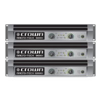
ODEPTHEORY:
MA-5000VZ
To
protect
the
output stages
from
adverse
thermal
conditions,
a
specially developed "ODEP" (Output Device Emulation Protection)
circuit
is
used.
It
produces
a
complex analog output signal proportional
to the
always changing safe operating
área
(SOÁ) margin
of the
output
transistors. This output
signal
controls
the
Voltage
Translatorstage
and
Low
Side output stage
bias.
This action removes only
the
drive that
may
exceed
the
safe-operating-area
of the
output stage.
Thermal sensors give
the
ODEP circuitry vital ¡nformation
on the
operating temperature
of the
heat sinks
on
which
the
output devices
are
mounted. This temperature signal combines with
the
complex ODEP
signal
to
form
the
heart
of the
patented ODEP protection scheme.
Ref
er
to
block
diagram
on the
next
page
for
a
discussion
of the
basic operation
of
the
ODEP system.
The
ODEP circuitry actually comes
¡n two
parts,
one
positive
and the
other
negative.
For the
purposes
of
discussion,
only channel
1
ODEP
circuitry
is
covered here,
and
focus
will
primarily
be on the
positive
half.
An
LM-334Z thermal sensor provides
a
calibrated output
from
the
output
modules.
At
25°C
its
output
is
2.98V, with
a
10mV
increase
per
every
1°C
rise
in
heatsink temperature.
This thermal sensor output, from the positive sensor, goes to
three
destinations. First
is a
buffer
which drives
the
calibrated temperature
test point
at pin 7 of
TP1/TP2.
Second
¡s an
over-temperature
limit
trip.
This will cause both
the
positive
and the
negative ODEP circuit
to go
into
and
remain
in
hard ODEP
until
the
heatsinks
cool.
Third,
it
goes down
into
a
circuit which combines thermal
and
output power
Information
for
proportional
fan
control
and,
whenneeded,
limiting.
The
thermal sensor
from
the
negative output module only
performs
this
last
function.
A
pair
of
sense
lines
from
the Low
Side emitter resistors provide current
information. Combined with
VCC
information actual instantaneous
power
¡s
calculated.
A
combining circuit determines
the net
thermal
12-MA-5000VZ
 Loading...