49 50
HOW TO CHECK THE P.C.B. ASS’Y
COURSE 1
Keep pushing three button (WASH, RINSE, SPIN SELECTOR) together and turn on the power switch.
COURSE2
Keep course 1 and pushing button of RINSE and SPIN
•RINSE BUTTON
•SPIN BUTTON
No. TIME DISPLAY FUNCTION
1 SEC State of first lighting.
Temperature which sensing thermistor.
2 SEC LO : Thermistor open.
HI : Thermistor short.
3 SEC All LED light 8 times and go back to first stage.
DISPLAY FUNCTION
drain`➜`off`➜`cold water`➜`off`➜`hot
water`➜`off`➜`pulsator
rotate(right)`➜`off`➜`bubble`➜`off`➜`pulsator
rotate(left)`➜`off➜pump➜`off`➜`fan`➜`off`➜`heater
`➜`off`➜`load check`➜`off`➜`door
check`➜`off`➜`all led light
TIME TO PUSH
DISPLAY FUNCTION
THE SPIN BUTTON
1st Time
2nd Time
3rd Time
drain
`➜`
spin
`➜`
cold water
`➜`
hot
water
`➜`
pulsator rotae(right)
➜
bubble
➜`
pulsator
rotae(left)
`➜
pump
`➜
fan
`➜`
heater
`➜`
door
check(dc/do)
`➜`
off
Repeat drive without “off” in “d2”
function
FUZ
FUZ
FUZ
WASH
MIN.
DRY HOT COLD
H.
M.
L.
S.
ES.
FUZ.
MEM.
SOAK.
SUIT.
SILK.
SPEE
STRO
NIGHT
BLAN
DRY
TIME
FEED RINS RES SPIN
TIME HOUR MIN. REM.
WASHSOAK
HOUR
MIN.
DRY HOT COLD
H.
M.
L.
S.
ES.
FUZ.
MEM.
SOAK.
SUIT.
SILK.
SPEE
STRO
NIGHT
BLAN
DRY
TIME
FEED RINS RES SPIN
TIME HOUR MIN. REM.
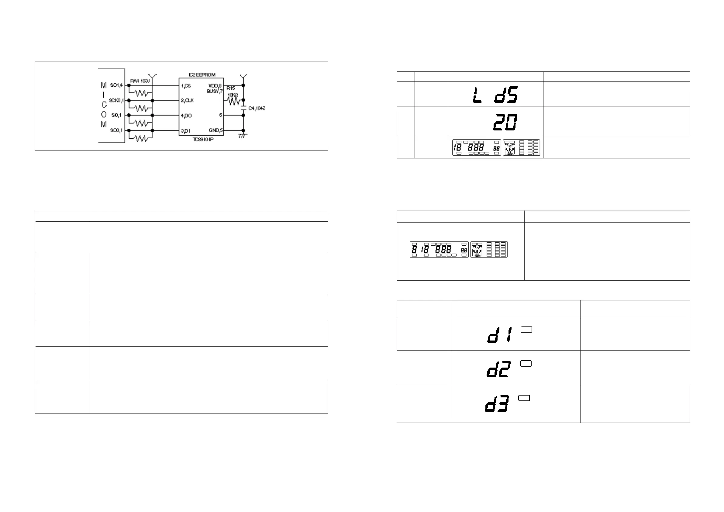
EEPROM UNIT
1. CIRCUIT DIAGRAM
2. EXPLANATION OF CIRCUIT
In contrast with mask ROM, EEPROM which enable WRITE/READ by program, memorize data even
during POWER is OFF.
• EEPROM PIN FUNCTION
EEPROM stores the selected contents in MEMORY course and LOAD SENSING data.
If you press MEMORY button, MICOM read the contents in MEMORY course and L.E.D displays the
selected contents in MEMORY course.
3. CAUTION FOR A/S
1. When the selected contents of MEMORY course in EEPROM can not memorize, EEPROM is
defective.
PIN NAME FUNCTION
Chip selector
CS Chip is enabled when CS is at ‘L’ level.
Set CS to ‘H’ level before executing instruction.
Clock input
CLK The DI data is latched at the rising edge of CLK.
The data is out from DO at the falling edge of CLK.
CLK is enable when CS is at ‘L’ level.
DI Serial data input
The address, command and data input pin.
DO Serial data output
The data output pin
Organization select
ORG The 16-bit organization is selected when ORG is ‘H’ level.
The 8-bit organization is selected when ORG is ‘L’ level.
Status output
RDY/BUSY ‘L’ level is output during program or chip eraise operation.
‘H’ level is output when program or chip eraise operation is completed.