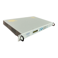
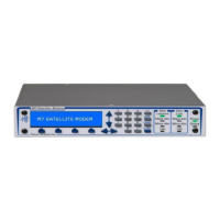
Installation PSM-500/500L/500LT SCPC Satellite Modem
Page 2-6 PSM-500/500L/500L T- Rev. 0.91
2.3.1 Data Interface Pin Connections
The unit is supplied with an electronically programmable data interface assembly. Table 2-1
shows the pin assignments for the possible standard interfaces. Additional information aiding the
creation of “adaptor” cables from the unit’s 37-pin female “D” sub connector to other types of
interface connections such as V.35 “Winchester” type connector standard pin-outs or RS-232
type DB25 connector is presented in Appendix C “Cabling Specifications”.
Table 2–1 Data Interface
Connector J3 Pin Assignment by Signal
Modem
Pin #
RS–449 Signal Name V.35, V.36 Signal
Name
RS-232 Signal Name
*(5)
Eia-530 Signal Name Direction
1 Shield (GND) Shield (GND) Shield (GND) SHD (GND) GND (4)
4 Transmit Data (A) – SD A (SD-)
SD
TD A Input
22 Transmit Data (B) + SD B (SD+)
TD B Input
5 Transmit Clock (A) – SCT A (ST-)
TTSETC A Output
23 Transmit Clock (B) + SCT B (ST+)
TSETC B Output
6 Receive Data (A) – RD A (RD-)
RD A Output
24 Receive Data (B) + RD B (RD+)
RD B Output
8 Receive Clock (A) – SCR A (RT-)
RSETC A Output
26 Receive Clock (B) + SCR B (RT+)
RSETC B Output
7 RTS (A) – RTS RTS RTS A Input
25 RTS (B) +
RTS B Input
9 CTS (A) – CTS
CTS A Output
27 CTS (B) +
CTS B Output
11 Data Mode (A) – DSR
DCR A Output
29 Data Mode (B) +
DCR B Output
12 TR (A) – DTR DTR DTR A Input
30 TR (B) +
DTR B Input
13 Receive Ready (A) – RLSD RLSD RLSD A Output
31 Receive Ready (B) +
RLSD B Output
17 Terminal Timing (A) – SCTE A (TT-)
TSETT A Input
35 Terminal Timing (B) + SCTE B (TT+) TSETT B Input
3 External data Clock
(transmit data clock or
receive FIFO Buffer
output Clock (A) – *(3)
Ext Data/FIFO Clock
A (-)*(3)
Ext Data/FIFO Clock
A (-)*(3)
Ext Data/FIFO Clock
A (-)*(3)
Input
21 External data Clock
(transmit data clock or
receive FIFO Buffer
output Clock (B) + *(3)
Ext Data/FIFO Clock
B (+)*(3)
Ext Data/FIFO Clock
B (+)*(3)
Ext Data/FIFO Clock
B (+)*(3)
Input
19 Signal GND SIG GND GND SGND GND
20 Common Chassis GND
10 Mod Fault Alarm *(2) Mod Fault Alarm *(2) Mod Fault Alarm *(2) Mod Fault Alarm *(2) OC TTL
output