Ri
x 2 Vrms = Resolver L-L rms voltage
Rf
Rf ≥ 6 kΩ
S1 and S3, S2 and S4, and RH and RL should be ideally twisted shielded, with the shield tied to GND at the converter.
Note : For 2v direct input use 10K Ω matched resistors for Ri & Rf.
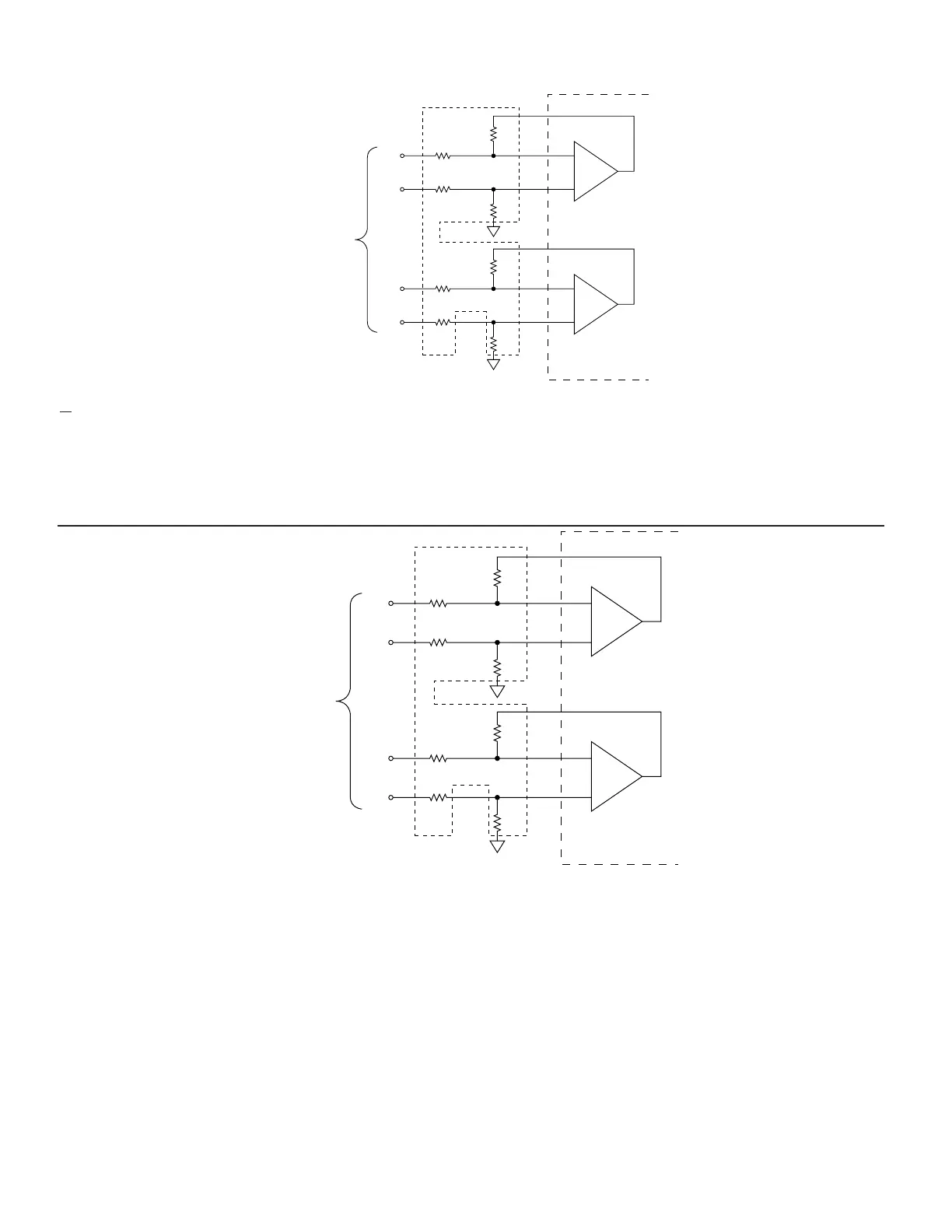
FIGURE 8A. DIFFERENTIAL RESOLVER INPUT
FIGURE 8B. DIFFERENTIAL RESOLVER INPUT, USING DDC-49530, DDC-57470 (11.8 V),
DDC-73089 (2V), OR DDC-49590 (90 V)
S1 and S3, S2 and S4, and RH and RL should be ideally twisted shielded, with the shield tied to GND at the converter.For DDC-49530
or DDC-57470: Ri = 70.8 kW, 11.8 V input, synchro or resolver. For DDC-49590: Ri = 270 kW, 90 V input, synchro or resolver. Maximum
addition error is 1 minute using recommended thin film package.
Note on DC Offset Gains: Input options affect DC offset gains and therefore affect carrier frequency ripple and jitter. Offsets gains
associated with differential mode, (offset gain for differential configuration = 1 + RF/RI) and direct mode (offset gain for direct config-
uration = 1), show differential will always be higher. Higher DC offsets cause higher carrier frequency ripple due to demodulation
process. This carrier frequency ripple because it is riding on the top of the DC error signal causes jitter. A higher carrier frequency vs
bandwidth ratio will help decrease ripple and jitter associated with offsets. Summary: R/D’s with differential inputs are more suscepti-
ble to offset problems than R/D’s in single ended mode. RD’s in higher resolutions, such as 16 bit, will further compound offset issues
due to higher internal voltage gains. Although the differential configuration has a higher DC offset gain, the differential configuration’s
common mode noise rejection makes it the preferred input option. The tradeoffs should be considered on a design to design basis.
Note: The five external BW components as
shown in FIGURE 1 and 2 are necessary
for the R/D to function.
Note: The five external BW components as
shown in FIGURE 1 and 2 are necessary
for the R/D to function.
 Loading...