ADV7623 Hardware Manual
Rev. 0 – March 2010 22 Confidential NDA required
Location Mnemonic Type Description
111 CGND Ground TVDD and CVDD Ground
112 RXA_C- HDMI Input Digital input clock Complement of port A
in the HDMI interface.
113 RXA_C+ HDMI Input Digital input clock True of port A in the
HDMI interface.
114 TVDD Power Receiver terminator supply voltage (3.3 V)
115 RXA_0- HDMI Input Digital input channel 0 complement of port
A in the HDMI interface.
116 RXA_0+ HDMI Input Digital input channel 0 true of port A in the
HDMI interface.
117 CGND Ground TVDD and CVDD Ground
118 RXA_1- HDMI Input Digital input channel 1 complement of port
A in the HDMI interface.
119 RXA_1+ HDMI Input Digital input channel 1 true of port A in the
HDMI interface.
120 TVDD Power Receiver terminator supply voltage (3.3 V)
121 RXA_2- HDMI Input Digital input channel 2 complement of port
A in the HDMI interface.
122 RXA_2+ HDMI Input Digital input channel 2 true of port A in the
HDMI interface.
123 HP_CTRLB Digital Output Hot Plug Detect for port B.
124 5V_DETB Digital Input 5 V detect pin for port B in the HDMI
interface.
125 DGND Ground Ground for DVDD
126 DVDD Power Digital supply voltage (1.8 V)
127 DDCB_SDA Digital I/O HDCP slave serial data ports B.
DDCB_SDA is a 3.3 V input/output that is
5 V tolerant.
128 DDCB_SCL Digital Input HDCP slave serial clock port B.
DDCB_SCL is a 3.3 V input that is 5 V
tolerant.
129 CVDD Power Receiver comparator supply voltage (1.8V)
130 CGND Ground TVDD and CVDD Ground
131 RXB_C- HDMI Input Digital input clock complement of port B in
the HDMI interface.
132 RXB_C+ HDMI Input Digital input clock true of port B in the
HDMI interface.
133 TVDD Power Receiver terminator supply voltage (3.3 V)
134 RXB_0- HDMI Input Digital input channel 0 complement of port
B in the HDMI interface.
135 RXB_0+ HDMI Input Digital input channel 0 true of port B in the
HDMI interface.
136 CGND Ground TVDD and CVDD Ground
137 RXB_1- HDMI Input Digital input channel 1 complement of port
MX25L3206EM2I-12G (DIGITAL : IC722)
ADV7623 Hardware Manual
Rev. 0 – March 2010 23 Confidential NDA required
Location Mnemonic Type Description
B in the HDMI interface.
138 RXB_1+ HDMI Input Digital input channel 1 true of port B in the
HDMI interface.
139 TVDD Power Receiver terminator supply voltage (3.3 V)
140 RXB_2- HDMI Input Digital input channel 2 complement of port
B in the HDMI interface.
141 RXB_2+ HDMI Input Digital input channel 2 true of port B in the
HDMI interface.
142 HP_CTRLC Digital Output Hot Plug Detect for port C.
143 5V_DETC Digital Input 5 V detect pin for port C in the HDMI
interface.
144 DDCC_SDA Digital I/O HDCP slave serial clock port C.
DDCC_SDA is a 3.3 V input/output that is
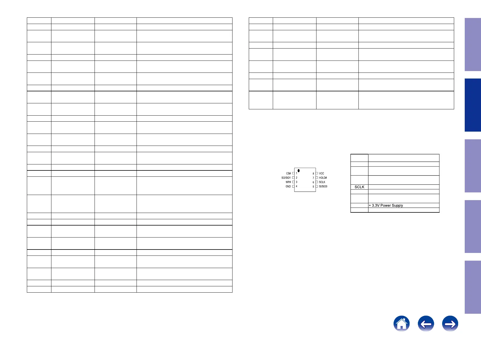
PIN CONFIGURATIONS
SYMBOL DESCRIPTION
CS# Chip Select
SI/SIO0
Serial Data Input (for 1 x I/O)/ Serial Data
Input & Output (for Dual Output mode)
SO/SIO1
Serial Data Output (for 1 x I/O)/ Serial Data
Output (for Dual Output mode)
Clock Input
WP# Write protection
HOLD#
Hold, to pause the device without
deselecting the device
VCC
GND Ground
PIN DESCRIPTION
8-PIN SOP (200mil)
37
Caution in
servicing
Electrical Mechanical Repair Information Updating

 Loading...