13
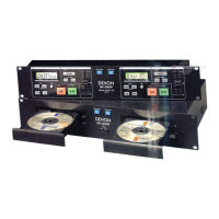
DN-S3500
85 P93 DSPRES_ O - Pd L L DSP RESET signal L: RESET
86 Vref+ Vref+ - - - - - Analog standard voltage +3.3V for AD conversion
87 AVDD AVDD - - - - - Power (+3.3V)
88 P94,DAC0 MSPD1 O - - - - MOTOR turn speed output D/A1
89 P95,DAC1 MSPD2 O - - - - MOTOR turn speed output D/A2(RESERVE)
90 P96,DAC2 MBRK O - - - - MOTOR BRAKE ON: H
91 P97,DAC3 LOAD O - - - - Disc loading, eject signal (D/A)
92 PC6,BREQ_ BREQ_ I - Pu - H Bus request signal
93 PC7,BRACK_ BRACK_ O - Pu H H Bus request accept signal
94 WEL_ WE_ O - Pu - H External memory write enable (lower 8bit)
95 P51 BOOT_ O - Pu H H DSP boot start signal L: START
96 RE_ RE_ O - Pu - H External memory read enable
97 CS2_ CS2_ O - Pu - H External memory chip select 2 (DSP Latch buffer interface)
98 VDD VDD - - - - - Power (+3.3V)
99 VSS VSS - - - - - GND
100 P54,BSTRE DACK_ I - Pu H H Not used
101 P55,WR_ DREQ_ O - Pu H H Not used
102 CS3_ CS3_ O - Pu - H Extended port chip select
103 A00 A00 O - - - - External memory address bus 0 (not used when 16bit bus select)
104 A01 A01 O - - - - External memory address bus 1
105 A02 A02 O - - - - External memory address bus 2
106 A03 A03 O - - - - External memory address bus 3
107 A04 A04 O - - - - External memory address bus 4
108 A05 A05 O - - - - External memory address bus 5
109 A06 A06 O - - - - External memory address bus 6
110 A07 A07 O - - - - External memory address bus 7
111 A08 A08 O - - - - External memory address bus 8
112 PD6 DSPF1 O - - L - FLAG1 for DSP
113 PD7,TM7IO DISCPB_ I - iPu - - Pulse B inverse count input for scratch DISC
114 A09 A09 O - - - - External memory address bus 9
115 A10 A10 O - - - - External memory address bus 10
116 A11 A11 O - - - - External memory address bus 11
117 A12 A12 O - - - - External memory address bus 12
118 A13 A13 O - - - - External memory address bus 13
119 VDD VDD - - - - - Power (+3.3V)
120 PC4 DSPF2 O - - L - FLAG2 for DSP
121 A14 A14 O - - - - External memory address bus 14
122 A15 A15 O - - - - External memory address bus 15
123 A16 A16 O - - - - External memory address bus 16
124 A17 A17 O - - - - External memory address bus 17
125 A18 A18 O - - - - External memory address bus 18
126 A19 A19 O - Pd - - External memory address bus 19
127 A20 A20 O - - - - External memory address bus 20
128 A21 A21 O - - - - External memory address bus 21
Pin
No.
Pin Name Symbol I/O DET Ext Ini Res Function
w
w
w
.
x
i
a
o
y
u
1
6
3
.
c
o
m
Q
Q
3
7
6
3
1
5
1
5
0
9
9
2
8
9
4
2
9
8
T
E
L
1
3
9
4
2
2
9
6
5
1
3
9
9
2
8
9
4
2
9
8
0
5
1
5
1
3
6
7
3
Q
Q
TEL 13942296513 QQ 376315150 892498299
TEL 13942296513 QQ 376315150 892498299
http://www.xiaoyu163.com
http://www.xiaoyu163.com