57
PIC24FJ256GA106 Terminal Functions
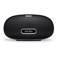
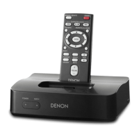
Model DSD300
Pin Port Name Description I/O Used I/O Note
1 RE5 NC I/O O/L No connect
2 RE6 SMBC I/O I/O Smbus Clock for Battery unit
3 RE7 SMBD I/O I/O Smbus Data for Battery unit
4 RG6 UART_BCO_TX0 I/O I UART TX for CX870
5 RG7 UART_BCO_RX0 I/O O UART RX for CX870
6 RG8 OLED_RST I/O O Reset for OLED. L: reset
7 _MCLR ICSPVPP-MCU I I Master Clear Input. This line is brought low to cause a Reset.
8 RG9 PWR_OLED12V I/O O Power control for OLED H: on
9 VSS GND P - Ground Reference for Logic and I/O Pin.
10 VDD VMCU1 P - Positive Supply for Peripheral Digital Logic and I/O Pin.
11 RB5 VER1 I/O I For destination setting Pin.
12 RB4 VER2 I/O I For destination setting Pin.
13 RB3 VER3 I/O I For destination setting Pin.
14 CN4 PWR_DET I I Power ON detect L: on
15 PGEC1 ICSPCLK I/O I Connect to Emulator (Programming Clock)
16 PGED1 ICSPDAT I/O I Connect to Emulator (Programming Data)
17 CN24 USB_FLG_DUCK I/O I Current detect of DOCK VBUS(INT). L:detect
18 RB7 AMP_NPDN I/O O Power Down for Amplier. L: Power down
19 VDD VMCU1 P - Positive Supply for Analog module.
20 VSS GND P - Ground Reference for Analog module.
21 CN26 AUX_IN_DETECT I/O I Connect detect of AUX Jack(INT). L:detect
22 RB9 USB_S2 I/O O VBUS control for Dock H: on
23 RB10 SPI_DSP_REQ I/O I Interrupt from DSP
24 RB11 AMP_POWER I/O O Power supply ON/OFF for Amplier. This Pin is not use.
25 VSS GND P - Ground Reference for Logic and I/O Pin.
26 VDD VMCU1 P - Positive Supply for Peripheral Digital Logic and I/O Pin.
27 RB12 LOUDNESS_SW I/O I Loudness Switch. H: on
28 RB13 IPOD5V_SW I/O O DC/DC on/off control (U16). H: on
29 RB14 MCU_TX1 I/O O Connect to Emulator
30 RB15 MCU_RX1 I/O I Connect to Emulator
31 SDA2 I2C_SDA2 I/O I/O I2C Data I/O for OLED
32 SCL2 I2C_SCL2 I/O O I2C Clock Out for OLED
33 RF3 SPI_NCS1 I/O O Not use
34 RF2 SPI_NCS2 I/O I/O Data for Serial Flash(U15)
35 CN72 IR2MCU1 I I IR Signal input Pin.
36 SDA1 I2C_SDA1 I/O I/O I2C Data I/O for RTC/Touch Key/Amp
37 SCL1 I2C_SCL1 I/O O I2C Clock Out for RTC/Touch Key/Amp
38 VDD VMCU1 P - Positive Supply for Peripheral Digital Logic and I/O Pin.
39 OSCI XTAL_32KI I I No Connect
40 OSCO XTAL_32KO O O No Connect
41 VSS GND P - Ground Reference for Logic and I/O Pin.
42 RD8 DSP_RESETOUT I/O I Reset Out of DSP. L: reset
43 RD9 ADSP_NRESET I/O O Reset for DSP. L: reset
44 RD10 ROM_RST I/O O Reset for Flash ROM. L: reset
45 RD11 CHGEN I/O O Battery Charge Enable L: enable
46 CN49 TOUCH_INT I I Interrupt from Touch Key Device.
47 RC13 MCU_RESET870 I/O O Reset of CX870 Module H: reset
48 RC14 AMP_NRESET I/O O Reset for Amplier. L: reset
49 RD10 SPI_CLK I/O O SPI Clock
50 RD2 SPI_MOSI I/O I SPI Data input from CX870
51 RD3 SPI_MISO I/O O SPI Data output to CX870