Nexys 3™ FPGA Board Reference Manual
Copyright Digilent, Inc. All rights reserved.
Other product and company names mentioned may be trademarks of their respective owners.
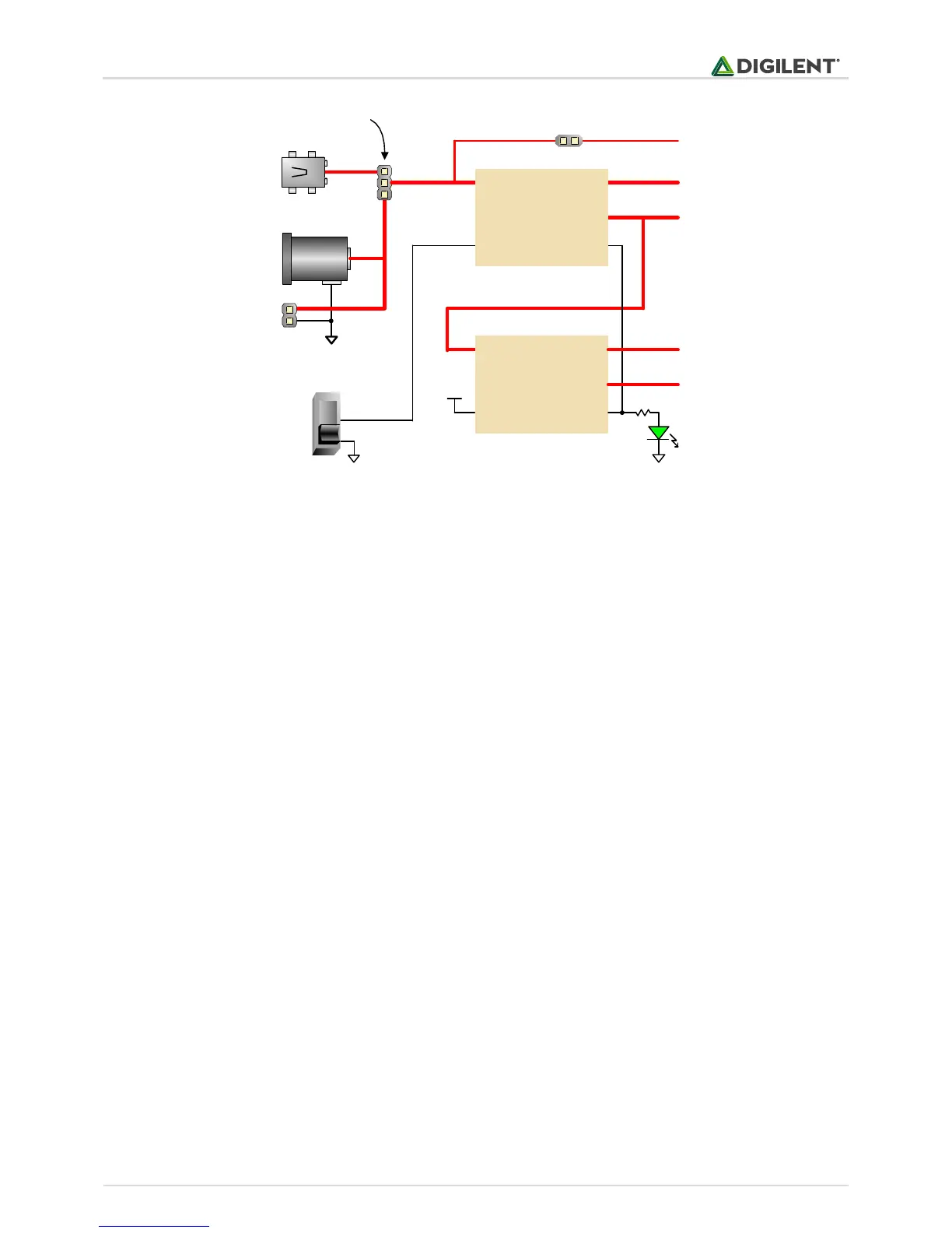
Power
Jack
Battery
Connector
Power Select
Jumper JP1
VU
1.8V
2.5V
1.2V
3.3V
IC13: LTC3633
EN
Power
Switch
Power On
LED (LD8)
IC15: LTC3619
ON
OFF
J11
Power GoodEN
3A
3A
400mA
800mA
USB port
Micro-USB
Power GoodEN
VUEXP
JP4
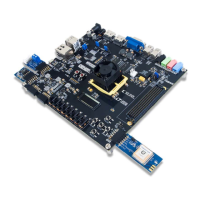
The Nexys 3 power supplies are enabled (or turned on) by a logic-level Power switch (SW8). A power-good LED
(LD8), driven by the wired-OR of the "power good" outputs on the supplies, indicates that all supplies are
operating within 10% of nominal.
The VU output of the main power jumper (JP1) is available to the VHDC expansion connector if jumper JP4 is
loaded. Care must be taken to ensure the VUEXP delivered to any attached expansion board is the correct voltage
– since VU is driven directly from an attached supply, this means a supply of the proper voltage must be used (e.g.,
5V).
3 Memory
The Nexys 3 board contains three external memories, all from Micron: a 128Mbit Cellular RAM (pseudo-static
DRAM); a 128Mbit parallel non-volatile PCM (phase-change memory); and a 128Mbit serial PCM device. The
Cellular RAM and parallel PCM device share a common bus, and the serial PCM is on a dedicated quad-mode (x4)
SPI bus. The non-volatile PCM memories are byte and bit alterable without requiring a block erase, so they are
faster and more versatile than conventional Flash in most applications.
The 16Mbyte Cellular RAM (Micron part number M45W8MW16) has a 16-bit bus that supports 8 or 16 bit data
access. It can operate as a typical asynchronous SRAM with read and write cycle times of 70ns, or as a synchronous
memory with an 80MHz bus. When operated as an asynchronous SRAM, the Cellular RAM automatically refreshes
its internal DRAM arrays, allowing for a simplified memory controller (similar to any SRAM controller). When
operated in synchronous mode, continuous transfers of up to 80MHz are possible.
The parallel PCM device (Micron part number NP8P128A13T1760E) is organized as 8Mwords of 16bits each. It
contains 128 individually erasable 64K-blocks, one of which is subdivided into four 16K "parameter blocks" that can
offer increased data protection. Normally, a device with a parameter block at the high end of the address space is
loaded (a "top parameter" block device). The parallel PCM memory offers 115ns read cycle times, with 25ns page-
mode reads within blocks. It has an internal 64-byte write buffer that can be written with 50ns cycle times, and the
64-byte buffer can be transferred to the Flash array in 120us (typical). The parallel PCM device also contains an SPI