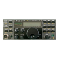
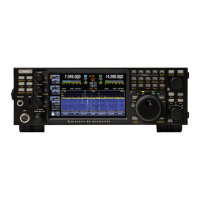
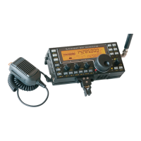
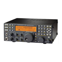
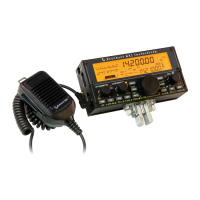
ELECRAFT 27
Uninstalled Components
Check off each of the components in the list below, verifying
that they are not yet installed.
__ C4, .01 (103) __ C5, .01 (103) __ C6, .01 (103)
__ C7, .01 (103) __ C8, .01 (103) __ R13, 68 k, 1%
__ RP3, 10 k resistor network
__ Q3, 2N3906
__ P1 (Mic. Configuration connector, on the bottom of the board)
The unfilled locations (above) are for parts that are provided
with the SSB adapter (model KSB2). If you have the SSB adapter
kit, you should install them now. Follow the third and fourth
assembly steps under Front Panel Board Components in the
KSB2 manual (page 16).
Visual Inspection
Make sure there are no components installed backwards. Check
all diodes, resistor networks, electrolytic capacitors, and ICs. The
parts placement drawings in Appendix F will be helpful in verifying
the orientation of diodes.
Examine the bottom of the PC board for solder bridges, cold
solder joints, or unsoldered components.
Resistance Checks
Set all potentiometers to their mid-points (approx.).
Perform the resistance checks (to ground) listed below. U1 is
on the back of the board.
Test Point Signal Name Res.
to GND
U1 pin 1 IDAT 25 - 35 k
U1 pin 2 ICLK 25 - 35 k
U1 pin 3 /SYNC 40 - 60 k
U1 pin 4 CLK > 50 k
U1 pin 5 5A 15 - 40 k
U1 pin 6 - 11 Ground 0
U1 pin 12 2V 9 - 11 k
U1 pin 13 - 40 LCD segments > 50 k
J1 pin 1 AF gain 1 > 1 M
J1 pin 2 AF gain 2 > 1 M
J1 pin 3 AF gain 3 > 1 M
J1 pin 4 DOT/PTT > 1 M
J1 pin 5 MIC AF > 1 M
J1 pin 6 ENC B > 50 k
J1 pin 7 AUXBUS > 1 M
J1 pin 8 Ground 0
J1 pin 9 SR DOUT > 50 k
J1 pin 10 SR DIN > 50 k
J1 pin 11 SR WRT > 50 k
J1 pin 12 SR CK > 50 k
J1 pin 13 ENC A > 50 k
J1 pin 14 SR RD > 50 k
J1 pin 15 VPOTS 10 - 60 k
J1 pin 16 ICLK 25 - 35 k
J1 pin 17 IDAT 25 - 35 k
J1 pin 18 5A 15 - 40 k
J1 pin 19 RF gain 1.5 - 3.5 k
J1 pin 20 Ground 0