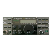
68 ELECRAFT
i
If you have already purchased option kits, you may install
selected option components now, as explained in the following
steps. This will simplify installation of the options after K2
alignment and test have been completed.
Do not remove the option bypass jumpers (W1, W2, etc.).
The K2 must be aligned and tested before the jumpers are
removed and option modules installed.
K160RX Component Installation (optional)
Locate the Installation section of the K160RX kit manual.
Cross out the first three steps (turning off the K2, removing
hardware, etc.), which are not applicable since the K2 is already
disassembled. Skip the next two steps. Do not remove W1.
Complete the steps for J14 through C13 and C14.
Cross out the next two steps (examination of Q7 and Q8).
The remaining steps should be completed after alignment.
KSB2 Component Installation (optional)
Locate KSB2 Module Installation in the KSB2 manual.
Complete only the steps required to install J11, J9, and J10,
and the standoff. Do not remove W2, W3, or C167 at this
time. Complete the remaining steps after alignment.
Other Option Component Installation (optional)
If you have the KAT2 (ATU) or KPA100 (Amplifier) option,
install 2-pin connector P6. Use the option manual's instructions.
If you have the KBT2 (Battery) or KPA100 option, install
2-pin connector P3. Use the option manual's instructions.
If you have the K60XV (60 meter) option, follow the
instructions in the K60XV manual under "Pre-Installation During
K2 Assembly".
If you have the KNB2 (Noise Blanker) option, locate the
Installation section of the KNB2 manual. Complete only the
installation of J12 and the standoff. Do not remove W5, R88,
R89 or R90 at this time.
Visual Inspection
Examine the bottom (solder side) of the RF board carefully for
unsoldered pins, solder bridges, or cold solder joints. Since this is a
large board, you should break the examination up into three parts:
__ perimeter area __ front half __ back half
Examine the top (component side) of the RF board for
unsoldered pins, solder bridges, or cold solder joints. This step is
necessary because some components are installed on the bottom of
the board and soldered on top.
Make sure switch S1 on the RF board is in the OFF position.
(Plunger OUT is OFF.)
Resistance Checks
Perform the following resistance checks.
Test Point Signal Name Res.
to GND
Q7 collector 12V > 500 ohms
Q6 base Driver bias 100-140 ohms
Q7 base PA bias 2.5 - 3.0 k
U11 pin 8 8A > 250 ohms
U10 pin 8 8 T > 500 ohms
U12 pin 1 8R > 500 ohms