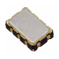
RX8900 SA / CE
Page - 12 ETM45E-01
VLF
Data Description
Write
0 The VLF bit is cleared to zero to prepare for the next status detection.
1 This bit is invalid after a "1" has been written to it.
Read
0
Data loss is not detected.
1
Data loss is detected. All registers must be initialized.
( This setting is retained until a "zero" is written to this bit. )
5) VDET ( Voltage Detection Flag ) bit
This flag bit indicates the status of temperature compensation. Its value changes from "0" to "1" when stop the
temperature compensation, such as due to a supply voltage drop. Once this flag bit's value is "1", its value is
retained until a "0" is written to it.
When after powering up from 0 V this bit's value is "1".
VDET
Data Description
Write
0 The VDET bit is cleared to zero to prepare for the next low voltage detection.
1 The write access of "1" to this bit is invalid.
Read
0
Temperature compensation is normal.
1
Temperature compensation is stop detected.
8.2.7. Control register
Address Function bit 7 bit 6 bit 5 bit 4 bit 3 bit 2 bit 1 bit 0
0F, 1F
Control Register CSEL1 CSEL0 UIE TIE AIE
RESET
(Default) (0) (1)
() () ()
(0) (0)
()
1)The default value is the value that is read (or is set internally) after powering up from 0 V.
2)"o" indicates write-protected bits. A zero is always read from these bits.
3)"" indicates no default value has been defined.
This register is used to control interrupt event output from the /INT pin and the stop/start status of clock and
calendar operations.
1) CSEL0,1 ( Compensation interval Select 0, 1 ) bits
The combination of these two bits is used to set the temperature compensation interval.
CSEL0,1
CSEL1
(bit 7)
CSEL0
(bit 6)
Compensation interval
Write/Read
0 0 0.5 s
0 1 2.0 s
Default
1 0 10 s
1 1 30 s
2) UIE ( Update Interrupt Enable ) bit
When a time update interrupt event is generated (when the UF bit value changes from "0" to "1"), this bit's value
specifies if an interrupt signal is generated (/INT status changes from Hi-Z to low) or is not generated (/INT status
remains Hi-Z).
When a "1"is written to this bit, an interrupt signal is generated (/INT status changes from Hi-Z to low) when an
interrupt event is generated.
When a "0"is written to this bit, no interrupt signal is generated when an interrupt event occurs.

 Loading...