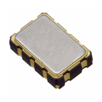
RX8900 SA / CE
Page - 2 ETM45E-01
3. Terminal description
3.1. Terminal connections
RX8900SA
1. T1 (CE)
14. N.C.
2. SCL 13. SDA
3. FOUT 12. T2 (V
PP)
4. N.C. 11. GND
5. V
BAT 10. / INT
6. V
DD 9. N.C.
7. FOE 8. N.C.
SOP14
in
RX8900CE
1. FOE
10. / INT
2. V
DD 9. GND
3. V
BAT 8. T2 (VPP)
4. FOUT 7. SDA
5. SCL 6. T1
(CE)
3.2. Pin Functions
Signal
name
I/O Function
SDA I/O
This pin's signal is used for input and output of address, data, and ACK bits, synchronized
with the serial clock used for I
2
C communications.
Since the SDA pin is an N-ch open drain pin during output, be sure to connect a suitable
pull-up resistance relative to the signal line capacity.
SCL Input This is the serial clock input pin for I
2
C Bus communications.
FOUT Output
This is the C-MOS output pin with output control provided via the FOE pin.
When FOE ="H"(high level), this pin outputs a 32.768 kHz signal.
When output is stopped, the FOUT pin = "Hi-Z"( high impedance ).
FOE Input
This is an input pin used to control the output mode of the FOUT pin.
When this pin's level is high, the FOUT pin is in output mode. When it is low, output via the
FOUT pin is stopped.
/ INT Output
This pins is used to output alarm signals, timer signals, time update signals, and other
signals. This pin is an open drain pin.
VBAT
This is a power supply pin for backup battery.
This is a pin to connect a large-capacity capacitor, a secondary battery.
When the battery switchover function does not need, VBAT must be connected to VDD.
VDD
This pin is connected to a positive power supply.
GND
This pin is connected to a ground.
TEST Input Use by the manufacture for testing. ( Do not connect externally.)
T1 (CE) Input Use by the manufacture for testing. ( Do not connect externally.)
T2 (VPP)
Use by the manufacture for testing. ( Do not connect externally.)
N.C.
This pin is not connected to the internal IC.
Leave N.C. pins open or connect them to GND or V
DD.
Note: Be sure to connect a bypass capacitor rated at least 0.1 μF between VDD and GND.

 Loading...