Do you have a question about the GOWIN GW1NSR-4C and is the answer not in the manual?
Illustrates the functional connections and data flow of the board.
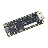
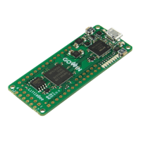
Details the technical specifications and parameters of the development board.
Provides information and references for the FPGA device used.
Introduces the methods for downloading code and debugging the FPGA.
Details the USB interface connection for downloading and debugging.
Explains the connection procedure for the J-LINK debugger.
Step-by-step instructions for downloading code and debugging.
Describes the power input and voltage regulation system.
Details the pin assignments for power supply connections.
Introduces the clock source and reset mechanism for the FPGA.
Lists pin assignments for the clock and reset signals.
Details the pin assignments for the board's LEDs.
Details the pin assignments for the key input.
Guidelines for safe handling, including electrostatic discharge prevention.
Guidance on using Secure FPGA mode and managing authentication codes.
| Series | GW1NSR |
|---|---|
| Logic Cells | 4608 |
| Operating Voltage | 1.2V |
| Operating Temperature | -40°C ~ 85°C |
| Mounting Type | Surface Mount |