11 Drawings
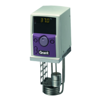
Fig 1
Fig 2
Fig 3
Fig 4
Fig 5
Fig 6
Fig 7 - 20
Circuit Diagram Power Supply
Circuit Diagram Display
Component Layout Power Supply Board
Component Layout Display Board
Wiring Diagram GD100 and GD120
Wiring Diagram GD100L and GD120L
Mechanical Diagrams
Temperature ºC Resistance W
0 1000.0
5 1019.5
10 1039.0
15 1058.5
20 1077.9
25 1097.3
30 1116.7
35 1136.1
40 1155.4
45 1174.7
50 1193.9
55 1213.2
60 1232.4
65 1251.6
70 1270.7
75 1289.8
80 1308.9
85 1328.0
90 1347.0
95 1366.0
100 1385.0
12 Probe Resistance Values
GD100/GD120
Part No. 17592/Issue 1 July 2002
Page 18