TMP92FD28
2007-01-30
92FD28-8
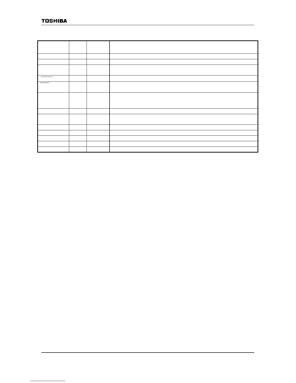
Table 2.2.1 Pin Names and Functions (3/3)
Pin name Number
of Pin
I/O
Function
X1 / X2 2 I/O High-frequency oscillator connection I/O pins
XT1 / XT2 2 I/O Low-frequency oscillator circuit connection pin.
AM0, AM1 2 Input Operation mode:
Fixed to AM1
“1” and AM0 “1”
RESET
1 Input Reset: Intializes TMP92FD28 (Schmitt input, with pull-up register)
PWE 1 Output External power supply control output: Pin to control ON/OFF of external power supply. In
stand-by mode, outputs “L” level. In other than stand-by mode, outputs “H” level.
D+, D- 2 I/O
Data pin connected to USB.
In case USB is not used, connect both pins to pull-up(DVCC3A) or pull-down resistor for
protect current flows it.
RVIN 2 Input Power supply pin for Internal Regulator
RVOUT1,
RVOUT2
2 Output 1.5V output from Internal Regulator (Only Mask ROM Version)
DVCC3A 5
í
Power supply pin for peripheral I/O-A (Connect all DVCC3A pins to power supply pin.)
DVCC3B 1
í
Power supply pin for peripheral I/O-B (Connect all DVCC3B pins to power supply pin.)
DVCC1A 1
í
Power supply pin for internal logic-A. (Only Mask ROM Version)
DVCC1B 1
í
Power supply pin for internal logic-B. (Only Mask ROM Version)
DVSS 8
í
GND pins (0 V) (All DVSS pins shold be connected with GND(0V))
Note1) In Flash version, the regulator does not built. But supply voltage as DVCC3 power because RVIN
pins are used power supply pins.
Note2) In Flash version, voltage does not output from RVOUT1 and RVOUT2.
Note3) When using MASK version in combination with Flash version, connect RVOUT1 and DVCC1B,
RVOUT2 and DVCC1A.
When using only Flash version, connect DVCC1A and DVCC1B, RVOUT1 and RVOUT2 to VDD3
 Loading...