5
BLOCK DIAGRAM DKG 972
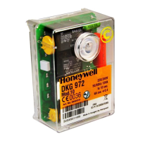
DKG 972
CIRCUIT AND TIMING DIAGRAM DKG 972
term. 8
term. 1
term. 9
blue
black
brown
IRD 1020.1
UVD 971
IRD- OR UVD CONNECTION
max. 10 A fast
6 A slow
Ph
IS
N
123456789 A
HS
ST RT EV
Z
V1
SA
Flame
amplifier
Reset
µC
Reset and
lock out
Power
supply
monitoring
13456789A
rz
rv1
rv2
rs
RZ
RV1 RV2 RS
Fault display
Information
system
EEPROM
Oscillator
tw tf tvz tn ts tv2
HS Mains switch
GW Gas proving switch
ST Limit thermostat
RT Control thermostat
EV External reset and lock out button
IS Ionisation probe
(IRD 1020.1, UVD 971see separate diagram)
Z Ignition
V1 Solenoid valve, 1st-stage
V2 Solenoid valve, 2nd-stage
SA External lock out signal
M Auxiliary blower
tw Waiting time
tf Stray light monitoring
tvz Pre-ignition time
tn Post-ignition
ts Safety time
tv2 2nd-stage delay
µC
Watchdog
Mains
monitoring
Power
supply
GW
V2
M
 Loading...