Table of Contents
Section
V
543. Input Attenuator Adjustments . . . . .
545. High
Frequency Phase
Adjustments
.
.
547.
High Frequency Log
AmplifierAdjustment
..........
549.
Factory Selected Components. .....
5-51. GencralServicinglnformation. .
. .. . .
5-5
3. Caurions
5-55. Assenbly Removal .
5-65. ComponentReplacement.
5-67. Servicing
Etched
Circuit
Boards. . .
.
.
5-70. Cleaningthe
Display
Window
......
5-72. Troubleshooting
.
.
. . .
5.74.
Cuidelines.
5-76. Syrnptoms.
5-78.
Tr,-rubleshool inB Trees.
5"82. MeasurementConditiotrs
5-84. Control Settings . .
5-86.
Power
Supply Troubleshooting
. . . . .
TABLE 0F C0NTENTS
(Cont'd)
Page
. .5.12
..5-12
.
.5-13
..5-14
..5-15
. .5.1 5
..5.15
.
.5.16
..5.16
..5.16
..5.18
..5.18
..5.18
..5-18
..5-18
..s-18
. .5.r 8
Section
VI
REPLACEABLE PARTS
6-1.
lntroduction
.... ..........6.1
64. Ordering Information . ......6-l
6-6. Non-Listed Parts . . . .
.......6-l
6'8. Proprietary Parts . . . . .......6-1
Model
3575A
Page
. . 5
-,i
..5-l
..5.E
APPENDICES
A. CODE LIST OF MANUFACTURERS
B.
SALES
AND
SERVICE OFFICES
C. BACKDATING
Figure
Page
l-1.
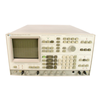
Model 3575A Gain-Phase Meter . . . . . . . . . . . . . . 1'0
2-1. Power
Cords ..........2-l
3-1. Front
Panel Description
...........3-2
3-2. Rear Panel Description
...........3-3
3-3. Power-Line
Ground Loop
.........3-3
34.
Source-Induced Ground Loop .... ...........34
3-5. Power lnput Module A, B
and C
.
. . . . . . . . . . . .3-j
3-6. dBV
to Volts Conversion ..........3-8
3-7. Worst
Case
Error Produced
by
Odd Harmonics .......3-9
3-8. Simple RC Network . .
.
. . . . . .
. . . . .3-9
3-9. Remote Pin
Connections .........3-12
3-10. Flag Timing
Delayed Mode .......3-14
3-1
1.
Flag
Timing
Non-Delayed
Mode .. . . . .. . . .. .3-14
4-1.
Simplified
Block
Diagram .........4-l
4-2.
Phase Difference
+
60 Degrees
. . . . . . . . . . . . . . . 44
4-3. Phase Detector
Output
.. ...
-....
.44
4-4. Phase Control
Filter
Output
. . . . . . . . . . . . . .
.
. 4-5
4-5. Basic Filter CDnfiguration
.........4-5
4-6. Phase
Control
Logic Functional Block
Diagram . ...
-....
..
.
-4-6
4-1. Logic Gates... -.......1-7
4-8. Aand BInPhase
-No
Distortion .
.
. .
. . . . .
.
. . . 4-8
,1-9.
Even Harmonics Cancelled
. .. . ... ..4-9
4-10. A and B Clean
-
No Error ..-.......4-9
4-11. l-arge
Error Produced
by
Noise . ...
-.. -......4-9
4-12.
Panel Meter Block Diagram
.
......4-11
4-13. Analog and
Digital Timing
...,,.4-13
Figure
4-14.
Timing Circuits and Functional
Block Diagram
5.1 . Power Splilter. . .
5-2.
Arnplitude and
Phase
Accuracy Checks
.
.
. . .
5-3. Shunt Capacitance Check
54. R/C Phase
Shifr
Network .
5-5.
Removing the Front Panel, Panel Meters
andAl2 . ........5-17
5-6.
Location
of Main Assemblies and
Adjustments ,...5-21/5-12
5-7-" Location of Panel Meter
Adjustments ... .5-2115-22
Amplitude
TroubleshootingTree ........5.23'5.:4
Dig.ital Panel Meter Troubleshooting Tree
.5-25/5-26
Phase Troubleshooting Tree .. .5.27'5.28
Phase l,ogic TroubleshootingTree
.......5-29/5-30
Mechanical Parts
(Main
Frame)
. . . . . . . . . . . . .
6.17
Mechanical
Parts
(Panel
Meter)
.
. .
. . . . . . . . . . 6- 1 9
Functional Block Diagram ......7-5
7-o
Preamplifier
(Al/A2)
and Log Converter
(A3/A4)
Schematics
and
Component Location
Diagrams .
........7-711-8
7-3. Phase Detector
(A5)
Schematic
and
Component Location Diagram . . . . . .
7
-9
l7
-10
7-4. Current Source
(46)
and Phase Control
Logic
(Al
1) Schematics
and Component Location Diagrams .....7-ll
17-12
7-5. Phase
Control
Filter
(A7)
Schematic
and Component l-ocation Diagram .....7-1317-14
LIST OF
ILL
USTBATIO NS
5-8.
5-9.
s-10.
5-11.
6.1 .
6-2.
'7-1.
7.2.
1V