The TVS is used to provide the ESD and surge protection due to a large number of SIM card operations.
9.4.7 I/O Interface Circuit
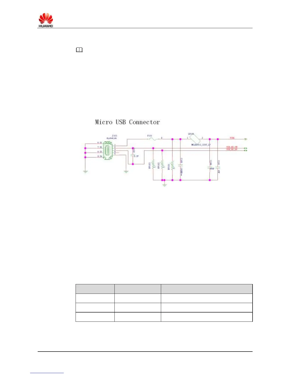
Circuit Diagram
Figure 9-39 shows the circuit diagram of the I/O interface.
Figure 9-39 Circuit diagram of the I/O interface
Analysis
When a charger is connected to the I/O interface, the charger provides the VCHG charging
voltage to charge the battery. When a data cable is connected to the I/O interface,
USB_HS_DN and USB_HS_DP are used for communication between the G510 and computer
(to upgrade the software and read the G510's information).
Troubleshooting
Fault symptom: The I/O interface is faulty, and the battery fails to be charged.
Handling: Clean, re-solder, or replace the interface.
Circuit Symbols