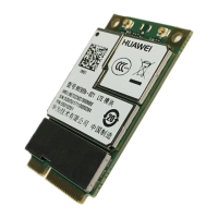
HUAWEI ME909s Series LTE Mini PCIe Module
Hardware Guide
Description of the Application Interfaces
Huawei Proprietary and Confidential
Copyright © Huawei Technologies Co., Ltd.
Mini PCI
Express
Standard
Description
P indicates power pins; I indicates pins for digital signal input; O indicates pins for digital
signal output. PO indicates power output pins; PI indicates power input pins.
V
IL
indicates Low-level Input voltage; V
IH
indicates High-level Input voltage; V
OL
indicates
Low-level Output voltage; V
OH
indicates High-level Output voltage.
The NC (Not Connected) pins are floating and there are no signal connected to these pins.
The Reserved pins are internally connected to the module. Therefore, these pins should not
be used, otherwise they may cause problems. Please contact with us for more details about
this information.
3.3 Power Interface
3.3.1 Power Sources and Grounds
For the Mini PCIe Adapter, +3.3Vaux is the only voltage supply that is available.
Table 3-2 Power and ground specifications
4, 9, 15, 18,
21, 26, 27,
29, 34, 35,
37, 40, 43,
and 50
 Loading...