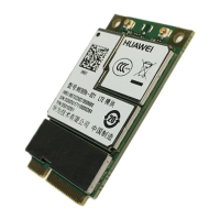
HUAWEI ME909s Series LTE Mini PCIe Module
Hardware Guide
Description of the Application Interfaces
Huawei Proprietary and Confidential
Copyright © Huawei Technologies Co., Ltd.
The rising time of VCC_3V3 should be 100 µs at least.
3.4 Signal Control Interface
3.4.1 Overview
The signal control part of the interface in the ME909s Mini PCIe module consists of
the following:
WAKE# signal
WAKEUP_IN signal
RESIN_N signal
LED_WWAN# signal
Table 3-3 lists the pins on the signal control interface.
Table 3-3 Definitions of the pins on the signal control interface
Open collector
active low signal.
This signal is
used to wake up
the host.
Sleep
authorization
signal.
H: Sleep mode is
disabled.
L: Sleep mode is
enabled (default
value).
The signal is
internally
pulled up.
 Loading...