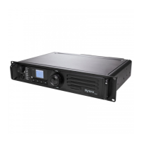
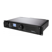
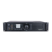
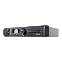
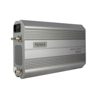
Service Manual
81
11 98_SYNCB I/10-bi Reset SS t counter
12 RX_CV ltage dRX CV vo etect
13 98_FS SSI AD9864
14 RX_PLL_Power_E supply (5N Power V/3.3V) enable for PLL
15 98_DOUTA 864 SSI AD9
16 98_PE AD9864 SPI enable
17 98_DOUTB AD9864 SSI
18 GND
gFor groundin
19 98_CLKOUT AD9864 SSI
20 GND
For grounding
21 GND
For grounding
22 98_PC AD9864 SPI clock
23 RX_PWR_EN ower suppl enable RX p y (9.1V/5V/3.3V)
24 98_PD 864 SPI datAD9 a
25 9V3A .3V voltageRX 9
26 TV Band-pass control voltage
Table 8-3 Interface between Baseband and RX Module
DB26 (J701) is used for further developm cribed in the table below: ent. Its definition is des
Pin No. Name Description
1NC
2 GND
3 DB26_GPIO
General I/O interface with function defined
through the CPS
4
4 SWB+
5 NC
6AGND
7 input, subject to CPS settingsTx Audio External MIC signal
8 RX Audio
RX filter/flat audio output;
The audio output type is subject to CPS settings.
9 GND
10 used for USB, USB of MMP10 D+ When this pin is