Chapter 2. Architecture and technical overview 45
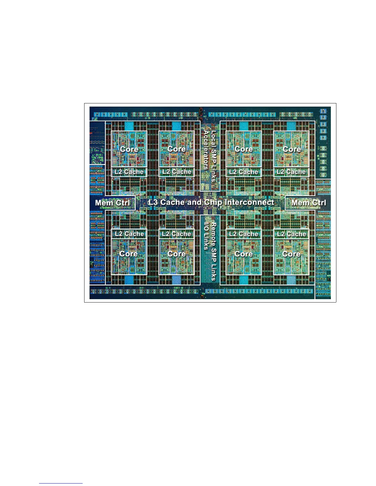
Figure 2-3 shows the POWER7+ processor die layout, with the major areas identified:
Processor cores
L2 cache
L3 cache and chip interconnection
Simultaneous multiprocessing links
Memory controllers.
I/O links
Figure 2-3 POWER7+ processor die with key areas indicated
2.1.1 POWER7+ processor overview
The POWER7+ processor chip is fabricated with IBM 32 nm Silicon-On-Insulator (SOI)
technology that use copper interconnects, and implements an on-chip L3 cache that use
eDRAM.
The POWER7+ processor chip is 567 mm
2
and has 2.1 billion components (transistors). Up
to eight processor cores are on the chip, each with 12 execution units, 256 KB of L2 cache
per core, and up to 80 MB of shared on-chip L3 cache per chip.
For memory access, the POWER7+ processor includes a double data rate 3 (DDR3) memory
controller with four memory channels.
 Loading...