Chapter 2. Architecture and technical overview 49
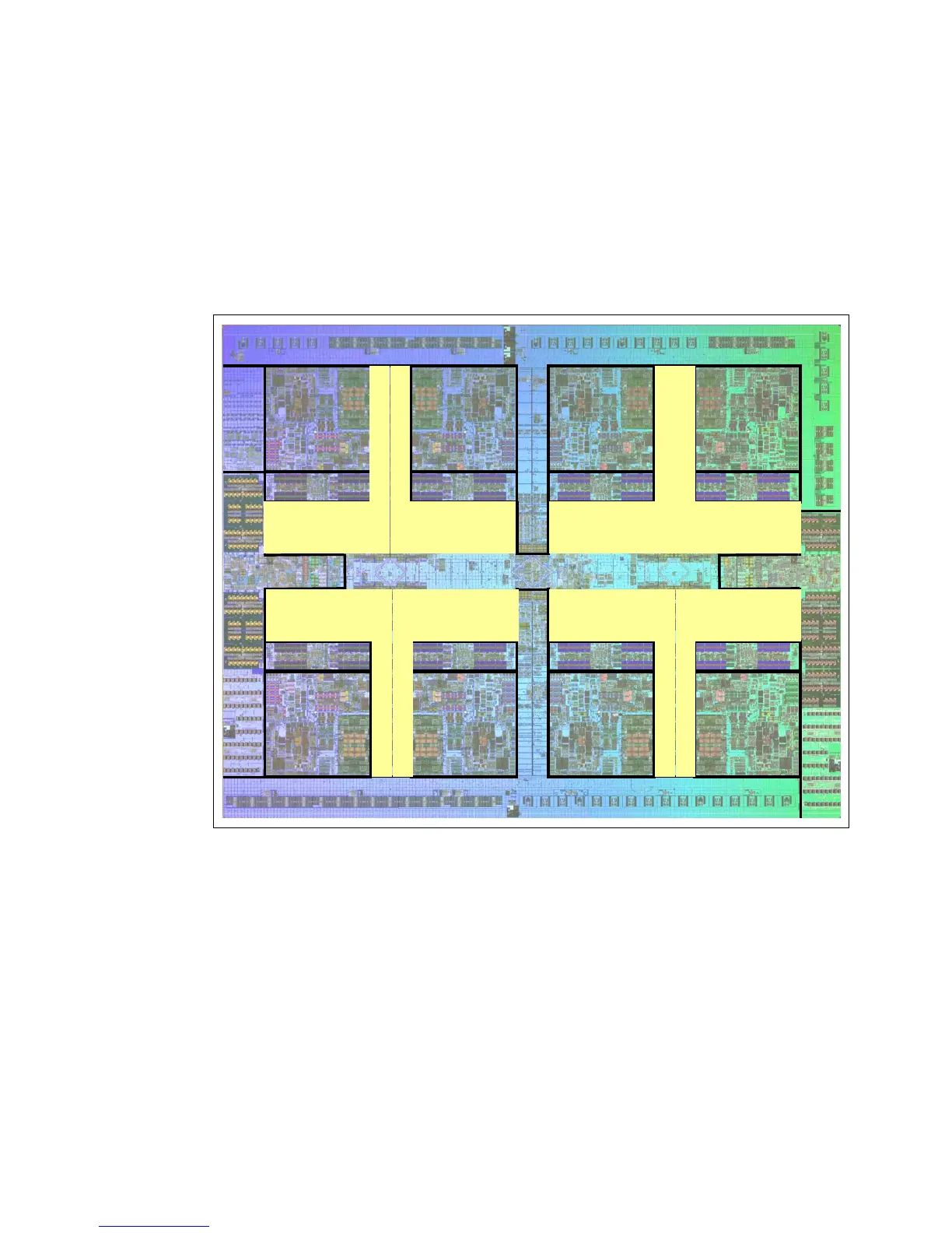
The on-chip L3 cache is organized into separate areas with differing latency characteristics.
Each processor core is associated with a fast local region of L3 cache (FLR-L3) but also has
access to other L3 cache regions as shared L3 cache. Additionally, each core can negotiate
to use the FLR-L3 cache associated with another core, depending on reference patterns.
Data can also be cloned to be stored in more than one core’s FLR-L3 cache, again depending
on reference patterns. This
Intelligent Cache management enables the POWER7+ processor
to optimize the access to L3 cache lines and minimize overall cache latencies.
Figure 2-6 shows the FLR-L3 cache regions for each of the cores on the POWER7+
processor die.
Figure 2-6 Fast local regions of L3 cache on the POWER7+ processor
The innovation of using eDRAM on the POWER7+ processor die is significant for
several reasons:
Latency improvement
A six-to-one latency improvement occurs by moving the L3 cache on-chip compared to L3
accesses on an external (on-ceramic) ASIC.
Bandwidth improvement
A 2x bandwidth improvement occurs with on-chip interconnect. Frequency and bus sizes
are increased to and from each core.
No off-chip driver or receivers
Removing drivers or receivers from the L3 access path lowers interface requirements,
conserves energy, and lowers latency.
Core Core Core Core
Core
L2 Cache
Core
L2 Cache
Core
L2 Cache
Core
L2 Cache
Mem Ctrl Mem Ctrl
L3 Cache and Chip Interconnect
Local SMP Links
Local SMP Links
Local SMP Links
Remote SMP + I/O Links
Remote SMP + I/O Links
Remote SMP + I/O Links
Fast local L3
Cache Region
Fast local L3
Cache Region
Fast local L3
Cache Region
Fast local L3
Cache Region
L2 Cache L2 Cache L2 Cache L2 Cache
Fast local L3
Cache Region
Fast local L3
Cache Region
Fast local L3
Cache Region
Fast local L3
Cache Region
 Loading...