Do you have a question about the Icom IC-2800 and is the answer not in the manual?
Critical safety precautions to prevent damage or injury during operation.
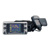
Details operating parameters, physical characteristics, and power requirements.
Technical specifications for transmitter output, receiver sensitivity, and selectivity.
Visual guide to component locations on the control unit PCB.
Visual guide to component locations on the main unit PCB.
Procedure for safely disassembling and removing the main unit from the chassis.
Procedure for safely disassembling and removing the control unit from the chassis.
Detailed explanation of receiver circuit functions and signal paths.
Specifics on the second IF stage and FM demodulation process using the FM IF IC.
Explanation of UHF circuits and overall transmitter circuit functions.
Details on VHF modulation, drive, and power amplifier circuits.
Description of Automatic Power Control (APC) and Phase-Locked Loop (PLL) systems.
Overview of the power supply system, including voltage lines and their regulation.
Mapping of CPU pins to specific functions and signals for control and data.
Essential preparation steps and a list of required test equipment for calibrations.
Diagram showing the correct hookup of test equipment for adjustments.
Procedures for adjusting PLL lock voltage, reference frequency, and transmitter output power.
Steps for calibrating receiver sensitivity and setting the S-meter function.
Procedures for adjusting squelch levels for both UHF and VHF bands.
Comprehensive list of part numbers and descriptions for the control unit.
Comprehensive list of part numbers and descriptions for the main unit.
List of mechanical components, chassis parts, main unit parts, and accessories.
Schematics and identification of transistors and diodes used in the device.
Top-view diagram showing component placement on the control unit PCB.
Bottom-view diagram showing component placement on the control unit PCB.
A comprehensive block diagram illustrating the overall system architecture and signal flow.
Diagram showing voltage distribution and supply points for the control unit.
| Brand | Icom |
|---|---|
| Model | IC-2800 |
| Category | Transceiver |
| Language | English |