Do you have a question about the Icom IC-290E and is the answer not in the manual?
Details semiconductor count, frequency coverage, resolution, control, readout, stability, memory, conditions, impedance, power, dimensions, and weight.
Details output power, emission mode, modulation system, deviation, spurious emission, carrier suppression, unwanted sideband, microphone, operating mode, and tone burst.
Details receiving system, mode, intermediate frequency, sensitivity, squelch sensitivity, spurious response, selectivity, audio output power, and impedance.
Overview of CPU control, band-edge detector, Endless System, frequency coverage, and applications.
Explains Memory Scan and Program Scan features, including adjustable speed and auto-stop.
Describes the use of two separate VFOs for simplex or duplex operation.
Details the LED display, tuning knob movement, automatic recycling, and step tuning.
Highlights RF amplifier, mixer circuits, MOS FETs, sensitivity, stability, and crystal filters.
Mentions built-in Noise Blanker, CW Break-in, CW Monitor, APC, and other features.
Instructions for carefully removing the transceiver from packaging and checking for shipping damage.
Guidance on placing the transceiver in a vehicle or fixed station for optimal use.
Details power source requirements (13.8V DC, 3.5A), negative ground system, and caution about excessive voltage.
Discusses the importance of a good, high-quality antenna for performance and impedance.
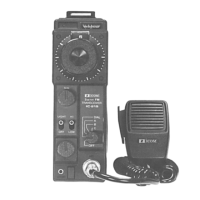
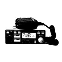
Details microphone, external speaker jack, impedance, and CW key connection and voltage.
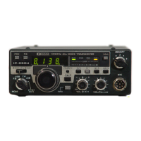
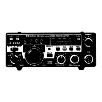
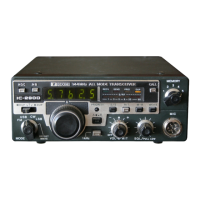
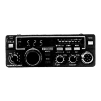
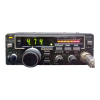
Identifies and describes front panel controls like RECEIVE INDICATOR, PRIORITY SWITCH, VFO SWITCH, etc.
Explains MODE switch for sideband selection and TUNING CONTROL KNOB for frequency adjustment.
Details selecting between VFO A/B and memory channels.
Explains 1KHz STEPS, VOLUME/POWER, RIT, SQUELCH/RF POWER, MIC, MEMORY, OFFSET, and AGC controls.
Describes NB, PRIORITY, SCAN, RIT, VFO/MEMORY, MEMORY/VFO WRITE, TONE CALL, and various indicators.
Explains S/RF indicator and rear panel connectors: ANTENNA, SPEAKER, KEY, POWER, ACCESSORY sockets.
Details SCAN SPEED, SCAN-STOP TIMER, SCAN-STOP TIME, VFO-SCAN FUNCTION, and SCAN-STOP FUNCTION controls.
General instructions for tuning and explains initial preset frequencies on display.
Shows how frequency display changes with MODE switch settings (FM, USB, CW, LSB).
Describes tuning frequency in steps, 1KHz STEPS SWITCH, and VFO/MEMORY/VFO SWITCH operation.
Explains VFO frequency transfer and RIT (Receiver Incremental Tuning).
Explains duplex operation and setting offset frequencies for repeaters.
Instructions for resetting the offset frequency for repeaters.
Step-by-step guide to programming memory channels using VFO A.
Explains how to recall frequencies from programmed memory channels.
Instructions for scanning Memory Channels and VFOs continuously.
Explains scanning between two programmed frequencies in Memory Channels 1 and 2.
Describes scanning the entire band between 144.000MHz and 145.999MHz.
Explains how scan modes restart after being stopped by auto-stop.
Further details on scan restart conditions based on timer and busy/empty channel settings.
Describes checking favorite channels while operating on a VFO.
Sets up knobs and switches for SSB reception, including mode selection and tuning.
Instructions for using the noise blanker for pulse type noise.
Explains AGC settings for SSB reception and transmitting procedures.
Sets up for CW reception, transmitting, and semi-break-in capability.
Explains the CW monitor circuit for side-tone adjustment.
Sets up for FM reception, including squelch adjustment.
Instructions for FM transmitting, simplex/duplex operation, and power settings.
Information on using satellites like AMSAT OSCAR 7 and 8, with frequency chart.
Identifies internal components and adjustment points on the main unit side.
Identifies internal components and adjustment points on the PLL unit side.
Overview of PLL circuit, microcomputer control, and receiver RF/IF stages.
Details detector, BFO, AF, AGC, and Noise Blanker circuits.
Explains the squelch circuit for silencing and the power supply regulator circuit.
Details antenna switching, microphone amplifier, FM modulator, and balanced modulator circuits.
Details various transmitter circuits including power amplifier, APC, and CW break-in.
Explains CW monitor, metering, and PLL unit local oscillator circuits.
Details mixer, filter, amplifier, programmable divider, and reference frequency generator circuits.
Details phase detector, loop filter, buffer amp, VCO, sensor, clock, and scan control circuits.
Describes the logic unit and the CPU control circuit.
Details CPU control flows related to mode switching and frequency steps.
Details CPU control flows for scan modes and offset write.
Details CPU control flows for scan modes and offset write.
Explains frequency control, display, and I/O circuits.
Describes the Digital to Analog converter circuit and logic unit block diagram.
Lists possible causes and solutions for power not coming on and no sound from the speaker.
Lists causes and solutions for low sensitivity and incomprehensible SSB reception.
Lists causes and solutions for no/low RF output and no modulation.
Lists causes and solutions for communication failures and lost memory frequencies.
Lists causes and solutions for scan function failures and electronic keyer problems.
Block diagram illustrating the main unit of the transceiver.
Block diagram illustrating the PLL unit of the transceiver.
Details optional accessories: IC-3PE AC Power Supply, BC-10A Memory Backup AC Power Supply, IC-CK1 DC Power Cord.
Details optional accessories: IC-SM5 Desk Microphone, IC-HM10 Scanning Microphone, IC-SP4 Mobile Speaker.
| Brand | Icom |
|---|---|
| Model | IC-290E |
| Category | Transceiver |
| Language | English |