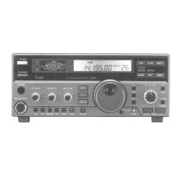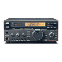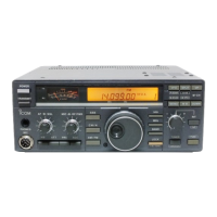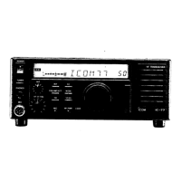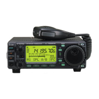


Do you have a question about the Icom IC-7200 and is the answer not in the manual?
| Brand | Icom |
|---|---|
| Model | IC-7200 |
| Category | Transceiver |
| Language | English |
Lists all components for the main unit.
Visual diagrams of PC board component layouts.
Schematic showing voltage distribution and connections.
Top-side component layout for the logic unit PC board.
Top-side component layout for the main unit PC board.
Top-side component layout for the RF unit PC board.
Top-side component layout for the VR-A unit board.
Top-side component layout for the VR-B unit board.
Top-side component layout for the MIC unit board.
Top-side component layout for the PHONE unit board.
Voltage distribution for Logic Unit 1.
Voltage distribution for Logic Unit 2.
Voltage distribution for the PA Unit.
Voltage distribution for the Main Unit.
Voltage distribution for the RF Unit.
Voltage distribution for the Filter Unit.
Details model, version, band, and carrier power specifications.
Guidelines for ordering replacement components.
Description of the RF circuit functions.
Description of the main unit circuits.
Description of the PA unit circuits.
Description of the filter unit circuits.
Block diagram showing voltage distribution.
Allocation and description of unit ports.
Required equipment and common connections for adjustment.
Procedures for transmitter and receiver adjustments.
Top-view layout of the logic unit PC board.
Top-view layout of the VR-A board.
Top-view layout of the VR-B board.
Top-view layout of the MIC board.
Top-view layout of the PHONE board.
Top-view layout of the RF unit PC board.
Top-view layout of the MAIN unit PC board.
Top-view layout of the FILTER unit PC board.
Top-view layout of the PA unit PC board.
Schematic diagram for the Logic Unit.
Schematic diagram for the VR-A board.
Schematic diagram for the VR-B board.
Schematic diagram for the MIC board.
Schematic diagram for the PHONE board.
Schematic diagram for the Main Unit.
Schematic diagram for the RF Unit.
Schematic diagram for the PA Unit.
Schematic diagram for the Filter Unit.