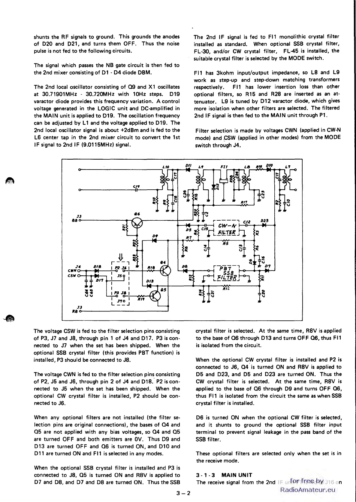
shunts the RF signals
to
ground. This grounds
the
anodes
of
020
and
021,
and turns them OFF. Thus
the
noise
pulse
is
not
fed
to
the
following circuits.
The signal which passes the
NB
gate circuit
is
then
fed
to
the 2nd mixer consisting
of
01
-
04
diode
OBM.
The 2nd local oscillator consisting
of
Q9 and
X1
oscillates
at 30.71901MHz . 30.720MHz with 10Hz steps.
019
varactor diode provides this frequency variation. A control
voltage generated
in
the
LOGIC unit and
~C-amplified
in
the
MAIN
unit
is
applied
to
019.
The oscillation frequency
can be adjusted by L 1 and
the
voltage applied
to
019.
The
2nd local oscillator signal
is
about +2dBm and
is
fed
to
the
L6
center
tap
in
the
2nd mixer circuit
to
convert
the
1st
IF
signal
to
2nd
IF
(9.0115MHz) signal.
elf
O----------------ill~--~~
416
J3
88~----------~~
J4
eWH
0-
.......
_.+----;-0
csw
O-+-
......
f-..,
J3
Df
R8~----------------------~
The voltage
CSW
is
fed
to
the
filter selection pins consisting
of
P3, J7 and JS, through pin 1
of
J4
and
017.
P3
is
con-
nected
to
J7 when
the
set has been shipped. When
the
optional
SSB
crystal filter (this provides PBT function)
is
installed, P3 should be connected
to
JS.
The voltage
CWN
is
fed
to
the
filter selection
pin~
consisting
of P2,
J5
and
J6,
through pin 2
of
J4
and O1S. P2
is
con-
nected
to
J5
when
the
set has been shipped. When
the
optional
CW
crystal filter
is
installed, P2 should be con·
nected
to
J6.
When any optional filters are
not
installed (the filter
se-
lection pins are original connections),
the
bases
of
04
and
05
are
not
applied with any bias voltages, so
04
and
05
are turned OFF and both emitters are
OV.
Thus
09
and
013
are turned OFF and
06
is
turned ON, and
010
and
011 are turned
ON
and
FI1
is
selected
in
any modes.
When
the
optional SSB crystal filter
is
installed and P3
is
connected
to
JS,
05
is
turned
ON
and
RSV
is
applied
to
07
and
OS,
and
07
and
OS
are turned ON. Thus
the
SSB
3-2
The 2nd I F signal
is
fed
to
FI1
monolithic crystal filter
installed as standard. When optional
SSB
crystal filter,
FL-30, and/or
CW
crystal filter, FL-45
is
installed,
the
suitable crystal filter
is
selected by the
MODE
switch.
FI1
has
3kohm
input/output
impedance, so
LS
and L9
work as step-up and step-down matching transformers
respectively.
FI1
has lower insertion loss than other
optional filters, so R15 and R2S are inserted
as
an at-
tenuator.
L9
is
tuned by
012
varactor diode, which gives
more isolation when other filters are selected. The filtered
2nd
IF
signal
is
then fed
to
the
MAIN
unit through P1.
Filter selection
is
made by voltages
CWN
(applied
in
CW-N
mode) and pSW (applied
in
other modes) from the
MODE
switch through
J4.
Itl!;
..
II<
DIO
D2J
crystal filter
is
selected. At
the
same time,
RSV
is
applied
to
the
base
of
06
through
013
and turns
OFF
06,
thus
FI1
is
isolated from
the
circuit.
When the optional
CW
crystal filter
is
installed and P2
is
connected
to
J6,
04
is
turned
ON
and
RSV
is
applied
to
05
and
023,
and
05
and
023
are turned ON. Thus
the
CW
crystal filter
is
selected. At the same time,
RSV
is
applied
to
the
base
of
06
through
09
and turns OFF
06,
thus
FI1
is
isolated from
the
circuit
the
same as when
SSB
crystal filter
is
installed.
06
is
turned
ON
when
the
optional
CW
filter
is
selected,
and it shunts
to
ground
the
optional
SSB
filter input
terminal
to
prevent signal leakage
in
the
pass band
of
the
SSB filter.
These optional filters are selected only when
the
set
is
in
the
receive mode.
3-1-3
MAIN
UNIT
The receive signal from
the
2nd I F unit
P1
is
fed
to
J16
on
for
free
by
RadioAmateur.eu