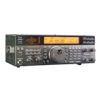
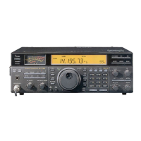
Do you have a question about the Icom IC-737 and is the answer not in the manual?
Important warnings to prevent damage and ensure safe operation of the transceiver.
Covers frequency range, mode, dimensions, weight, and environmental conditions.
Details output power, spurious emissions, carrier suppression, and impedance.
Covers receive system, intermediate frequency, sensitivity, selectivity, and RIT range.
Includes impedance range, minimum operating input, tuning accuracy, and insertion loss.
Step-by-step guide for safely removing the Power Amplifier (PA) block.
Procedure for safely detaching and removing the antenna tuner unit.
Diagrams illustrating the placement and identification of various connectors.
Visual identification of components on the main circuit board.
Identification of components on the PLL and Logic control boards.
Identification of components on the PA, Filter, and Elekey boards.
Explains RF switching, bandpass filter, mixer, and IF circuits within the receiver.
Describes transmitter/receiver interface and general transceiver operational circuits.
Explains frequency synthesis and control using Phase-Locked Loop (PLL) circuits.
Details the digital logic circuits responsible for control and sequencing.
Describes the impedance matching circuits for the antenna tuner.
Outlines the power supply voltage regulator circuits for stable distribution.
Lists required test equipment and initial checks before performing adjustments.
Step-by-step guide for adjusting PLL synthesizer parameters.
Procedures for adjusting receiver sensitivity, selectivity, and meter performance.
Guide for adjusting transmitter output power, gain, and keying timing.
Procedures for tuning and calibrating the antenna tuner for optimal performance.
Lists components and hardware mounted on the front panel of the unit.
Lists components and hardware for the main internal circuit board.
Lists components and hardware specific to the power amplifier section.
Lists components and hardware for the filter board.
Lists components and hardware for the logic control board.
Lists components and hardware for the antenna tuner.
Lists mechanical parts for the front panel, knobs, and overall housing.
Lists chassis components, screws, and included accessories.
Visual layout of components and connections on the main unit board.
Visual layout of components and connections on the logic unit board.
Visual layout of components and connections on the PLL unit board.
Layouts for AF, SW, Display, Jack, MIC, M-CH, and VR units.
Layouts for Control, SWR, and ANT-SW units.
Layouts for the Tune and Elekey units.
Layouts for the Filter and PA units.
Shows the functional blocks and signal flow within the FMAM unit.
Illustrates the functional blocks and interconnections of the main unit.
Depicts the functional blocks and signal paths of the logic unit.
Shows the functional blocks and signal flow within the control unit.
Illustrates the functional blocks and signal paths of the PLL unit.
Depicts the functional blocks and signal flow of the power amplifier unit.
Diagram illustrating voltage levels and distribution for the jack unit.
Diagram showing voltage levels and distribution for the AF unit.
Voltage diagrams for the front panel and display units.
Voltage diagrams for the filter and power amplifier units.
| Brand | Icom |
|---|---|
| Model | IC-737 |
| Category | Transceiver |
| Language | English |