


B
Barbara KennedyAug 20, 2025
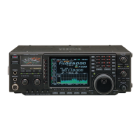
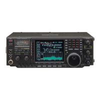
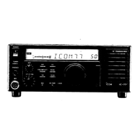
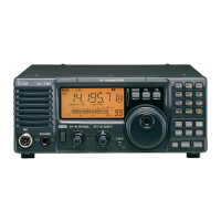
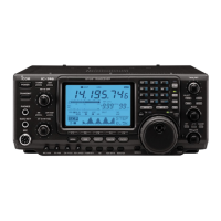
Why is the frequency not changing on my Icom IC-756PROIII Transceiver?
- DDavid BeltranAug 20, 2025
If the displayed frequency on your Icom Transceiver doesn't change properly, here are a few things to check: * Turn OFF the dial lock function by pushing [LOCK/SPEECH]. * Exit the set mode screen by pushing [EXIT/SET] several times. * Reset the CPU if it has malfunctioned.