


K
Kayla LeonSep 9, 2025
What to do if programmed scan does not start on Icom Transceiver?
- BBrandon GarrettSep 9, 2025
If your Icom Transceiver's programmed scan does not start, program different frequencies in scan edge memory channels P1 and P2.
What to do if programmed scan does not start on Icom Transceiver?
If your Icom Transceiver's programmed scan does not start, program different frequencies in scan edge memory channels P1 and P2.
How to fix Icom Transceiver when transmitting is impossible?
If transmitting is impossible on your Icom Transceiver, set the frequency to a ham band.
Why does the [ANT] switch not function on my Icom IC-756PROIII?
If the [ANT] switch on your Icom Transceiver does not function, set the antenna switch in set mode to 'Auto' or 'Manual.'
Why doesn't memory scan start on my Icom IC-756PROIII?
If memory scan does not start on your Icom Transceiver, program more than 2 memory channels.
Why doesn't select memory scan start on my Icom IC-756PROIII?
If select memory scan does not start on your Icom Transceiver, designate more than 2 memory channels as select channels for the scan.
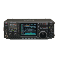
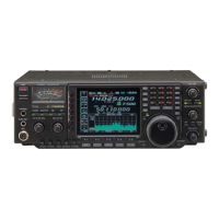
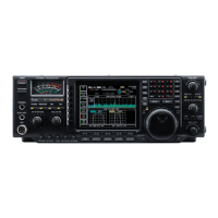
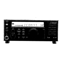
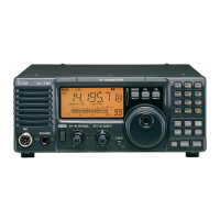
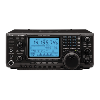
Describes the service information for the HF/50MHz ALL MODE TRANSCEIVER.
Lists critical safety warnings for operating and connecting the transceiver.
Details how to order replacement parts, including required information.
Provides essential guidelines and precautions for disassembling and repairing the transceiver.
Information about semiconductor components used in the transceiver.
Diagrams and lists of component locations on various internal boards.
High-level functional block diagram of the transceiver.
Diagrams illustrating voltage distribution across different units.
General specifications including frequency coverage, modes, power supply, dimensions, and display.
Specifications related to the transmitter output, modulation, spurious emissions, and connectors.
Specifications related to the receiver system, sensitivity, selectivity, and audio output.
Specifications for the internal antenna tuner, including impedance range and insertion loss.
Top view of the transceiver's internal layout with major circuit boards and components identified.
Bottom view of the transceiver's internal layout with major circuit boards and components identified.
Description of the RF receiver circuit, including RF switching, bandpass filters, and pre-amplifiers.
Description of the 1st IF circuit filtering and amplification stages.
Explanation of the 2nd mixer circuit for converting the 1st IF to the 2nd IF signal.
Description of the noise blanker circuit's function to detect and suppress pulse-type noise.
Explanation of the 2nd IF circuit amplification and filtering before the 3rd mixer.
Description of the 3rd mixer circuit and the resulting 3rd IF signal.
Explanation of the DSP circuit's role in digital IF filtering, noise reduction, and demodulation.
Description of the twin PBT circuit for digitally shifting the IF filter center frequency.
Description of the AGC circuit's function to control receiver gain and maintain constant audio output.
Description of the S-meter circuit indicating received signal strength based on AGC voltage.
Description of the squelch circuit that mutes audio output when the signal is below a set level.
Description of the AF amplifier circuit amplifying audio signals for the speaker.
Explanation of the microphone amplifier circuit for boosting audio signals.
Description of the VOX circuit that sets transmitting conditions based on voice input.
Explanation of the DSP circuit's role in modulating signals for transmission.
Description of the speech compressor circuit to increase average talk power.
Details of IF amplifier and mixer circuits in the MAIN-A and RF-B units for frequency conversion.
Description of the RF circuit amplifying transmitting frequency for RF output.
Explanation of the low-pass filter circuit suppressing harmonic components.
Description of the ALC circuit controlling IF amplifier gain for constant RF power output.
Description of the APC circuit protecting power amplifiers from SWR and excessive current.
Description of the temperature protection circuit activating the cooling fan.
Description of the monitor circuit for checking voice characteristics.
Overview of the PLL unit's functions, including LO frequencies and VCO circuits.
Description of the 1st LO PLL circuit containing main and reference loops.
Description of the 2nd LO and reference oscillator circuits generating system clock and LO signals.
Description of the 3rd LO circuit generating digital signals for the MAIN-A unit.
Description of the marker circuit using divided DDS signals for marker generation.
Explanation of the T-network matching circuit and tuning motors for low SWR.
Description of SWR, reactance, and resistance detectors for tuner operation.
Description of the motor control circuit for tuning motors and relays.
Port allocation details for the antenna tuner CPU.
Explanation of the scope receiver circuit for producing IF signals for the spectrum scope.
Description of the sweep LO circuit generating signals for the spectrum scope function.
Power supply lines for the PA unit.
Power supply lines for the front unit.
Power supply lines for the MAIN-A unit.
Power supply lines for the CTRL-A and PLL units.
Data for band selection across different circuit units.
Port allocation details for the sub-CPU.
Port allocation details for the MAIN-CPU.
Port allocation details for input expanders on the DISPLAY board and MAIN-A unit.
Port allocation details for output expanders on the PLL unit.
Filter select signal outputs from CTRL-A board IC11.
Bandpass filter select signals from RF-B unit IC401.
Bandpass filter select signals from RF-B unit IC402.
Control signals for attenuators and RX antenna select from RF-B unit IC403.
Strobe signals for output expanders and antenna connector select from MAIN-A unit IC3653.
Squelch mute control, speaker ON/OFF, and chip select signals from MAIN-A unit IC3654.
Control signals for noise blanker, TX monitor audio select, and audio recorder output from MAIN unit IC3752.
Mode select signals and RF power control signals from MAIN-A unit IC3753.
List of necessary test equipment with their specifications and ranges for adjustments.
Diagram illustrating the required test equipment connections to the transceiver.
Procedure for adjusting the reference frequency.
Procedure for adjusting the LPL-A lock voltage.
Procedure for adjusting the VCO-A lock voltage.
Procedure for adjusting the 1LO-A output level.
Procedure for adjusting the LPL-B lock voltage.
Procedure for adjusting the VCO-B lock voltage.
Procedure for adjusting the 1LO-B output level.
Procedure for adjusting the 3LO output level.
Procedure for adjusting the idling current for the drive stage.
Procedure for adjusting the TX peak output.
Procedure for adjusting the overall transmitter gain.
Procedure for adjusting the IC APC (Automatic Power Control) circuit.
Procedure for adjusting HF band output power.
Procedure for adjusting 50 MHz band output power.
Procedure for adjusting FM deviation.
Procedure for adjusting AM carrier power.
Procedure for adjusting AM modulation.
Procedure for adjusting the receiver peak signal level.
Procedure for adjusting FM distortion.
Procedure for adjusting the mixer balance for optimal signal mixing.
Procedure for adjusting the overall receiver gain.
Procedure for adjusting the noise blanker function.
Procedure for adjusting the spectrum scope function.
Procedure for adjusting the SWR detector circuit.
Steps to enter the meter adjustment mode.
Procedures for adjusting the meter scale for various S-meter positions.
Procedures for adjusting the TX power meter scale for different output levels.
Procedures for adjusting the 50 MHz power meter scale.
Procedure for adjusting the ALC meter.
Procedure for adjusting the drive level meter.
Procedure for adjusting the SWR meter.
Procedures for adjusting the receiver meter and scope scale.
List of mechanical and electronic parts for the front unit, including lamps, sensors, and screws.
List of parts for the display unit.
List of parts for the ten-key unit.
List of parts for the mode unit.
List of parts for the PBT unit.
List of parts for the RIT unit.
List of parts for the phone unit.
List of parts for the key unit.
List of parts for the microphone unit.
List of parts for the PLL unit, including ICs and passive components.
List of parts for the PA unit, including transistors, diodes, and regulators.
List of parts for the memory unit, including ICs and connectors.
List of parts for the MAIN-A unit, including ICs, transistors, and resistors.
List of parts for the DSP-A unit, including ICs, resistors, and capacitors.
List of parts for the RF-B unit, including diodes, inductors, and resistors.
List of parts for the BPF-A unit.
List of parts for the PREAMP unit.
List of parts for the tuner-A unit, including ICs, motors, and relays.
List of parts for the CTRL-A unit, including ICs, transistors, and connectors.
List of chassis parts, including screws, shields, and sponges.
List of accessories including microphone, PCB, and fan.
List of mechanical parts for the front unit, including lamps, sensors, and screws.
List of parts for the display board, including resistors and shield cases.
List of parts for the PBT board, including resistors and encoders.
List of parts for the RIT board, including encoders.
List of parts for the phone board, including connectors and earth springs.
List of parts for the key board, including connectors and earth springs.
List of parts for the microphone board, including connectors and earth springs.
List of chassis parts, including earth springs, shield cases, and sponges.
List of accessories including microphone, PCB, and fan.
Diagrams and symbols for transistors and FETs used in the transceiver.
Diagrams and symbols for various diodes used in the transceiver.
Top view layout of the DISPLAY board with component placement.
Top view layout of the MODE board with component placement.
Top view layout of the PHONE board with component placement.
Top view layout of the KEY board with component placement.
Top view layout of the TEN-KEY board with component placement.
Bottom view layout of the DISPLAY board with component placement.
Top view layout of the MODE board with component placement.
Top view layout of the PHONE board with component placement.
Top view layout of the KEY board with component placement.
Top view layout of the TEN-KEY board with component placement.
Bottom view layout of the TEN-KEY board with component placement.
Bottom view layout of the PHONE board with component placement.
Bottom view layout of the KEY board with component placement.
Bottom view layout of the MODE board with component placement.
Top view layout of the PBT board with component placement.
Top view layout of the RIT board with component placement.
Top view layout of the MIC board with component placement.
Top view layout of the MEMORY board with component placement.
Bottom view layout of the MEMORY board with component placement.
Bottom view layout of the PBT board with component placement.
Bottom view layout of the MIC board with component placement.
Bottom view layout of the RIT board with component placement.
Top view layout of the MAIN-A unit with component placement and connector identification.
Bottom view layout of the MAIN-A unit with component placement.
Top view layout of the DSP-A board with component placement.
Bottom view layout of the DSP-A board with component placement and connector identification.
Top view layout of the RF-B unit with component placement and connector identification.
Bottom view layout of the RF-B unit with component placement.
Top view layout of the BPF-A board with component placement.
Top view layout of the PREAMP board with component placement.
Bottom view layout of the PREAMP board with component placement.
Bottom view layout of the BPF-A board with component placement.
Top view layout of the PLL unit with component placement and connector identification.
Bottom view layout of the PLL unit with component placement.
Top view layout of the PA unit with component placement and connector identification.
Bottom view layout of the PA unit with component placement.
Top view layout of the FILTER-A unit with component placement and connector identification.
Bottom view layout of the FILTER-A unit with component placement.
Top view layout of the CTRL-A unit with component placement and connector identification.
Bottom view layout of the CTRL-A unit with component placement.
Top view layout of the TUNER-A board with component placement and connector identification.
Bottom view layout of the TUNER-A board with component placement.
Overall block diagram showing the interconnection of major functional units and circuits.
Voltage distribution diagram for the front unit.
Voltage distribution diagram for the DSP-A board.
Voltage distribution diagrams for the tuner-A, memory, and CTRL-A units.
Voltage distribution diagram for the MAIN-A unit.
Voltage distribution diagram for the PLL unit.
Voltage distribution diagrams for the PA and FILTER-A units.
Voltage distribution diagram for the RF-B unit.
| Brand | Icom |
|---|---|
| Model | IC-756PROIII |
| Category | Transceiver |
| Language | English |