3 - 9
3-5 CPU PORT ALLOCATIONS
Pin
No.
Line
Name
Description I/O
5–20
H8_A0–
H8_A13
DSP address bus. O
21 UNLKA
PLL unlock detect signal input for VCO-A.
H=Unlock detected.
I
22 UNLKB
PLL unlock detect signal input for VCO-B.
H=Unlock detected.
I
23 ECK EEPRROM (HN58X2464TI) clock. O
24 EDT EEPRROM (HN58X2464TI) data. I/O
26 USCK USB HUB (USB2502) clock. O
27 USDA USB HUB (USB2502) data. O
28 UPWS
USB HUB (USB2502) power control.
H=USB power ON.
O
29 VBUS
VBUS connection detect for USB HUB
(USB2502).
H=USB connection detected.
I
30 RTKI
RTTY keying input.
H="Space" input.
I
31 TRVI
Transverter input (from [ACC2]).
L=A transverter is connected.
I
33 SDAT Scope DDS/PLL/DSP data. O
34 SST2 Scope PLL(ADF4630-8) strobe. O
35 EXRL1
External SEND reray output.
H=Relay ON
O
36 EXRL2
External SEND reray output.
H=Relay ON
O
37
H8_
CS6#
Dual-port SRAM chip select signal.
L=Selected.
O
38
H8_
CS7#
Expander chip select signal.
L=Selected.
O
42
PCK/
CON0
DDS clock. O
43
PDAT/
CON1
DDS data. O
44 CON2 DDS mode control. O
45 PSL PLL strobe. O
46 METV
External meter voltage.
(PWM, 7800 Hz, 12 bit resolution)
O
47 PST PLL strobe output. O
48 ESTA
External tuner "START" signal output.
L=Tuning start.
O
49 EKEY
External tuner "KEY" signal input.
L=While tuning/tune NG.
I
51 MCK Scope PLL clock. O
52 MDAT Scope PLL data. O
53 TCON External tuner conection detect. I
54 CTXD CI-V (UART) output. O
55
CRXD/
CBSY
CI-V (UART) input/CI-V bus busy input.
L=Data "1" /Busy.
I
56 DSPCK DSP clock. O
57 DSPR DSP data. O
59 SST1
Chip select signal for scope DDS (AD9834).
L=Selected.
O
60 SPS0
Scope DDS (AD9834) frequency register
shift signal.
O
61 SCK Scope DDS/PLL/DSP clock. O
63-
80
H8_D0-
H8_D15
DSP data b
us
. I/O
81 RTD DSP RTTY/BPSK/QPSK (H) decode data. I
82 TND QPSK (L) decode data. I
Pin
No.
Line
Name
Description I/O
83 NSQ Input noise pulse. I
84
H8_
WAIT#
Bus control "Wait" signal. I
85 TRAS SEND signal. O
87
H8_
LWR#
(Bus control) "L" write signal.
L=While writing.
O
88
H8_
HWR#
(Bus control) "H" write signal.
L=While writing.
O
89
H8_
RD#
(Bus control) Read signal.
L=While reading.
O
90 H8_AS# (Bus control) Adress strobe. O
94 SENI
PTT/ACC SEND signal.
H=While transmitting.
I
104 CTFL CW TX status. I
105 RXS
RX circuits power ON.
L=While receiving.
O
106 TXS
TX circuits power ON.
L=While transmitting.
O
107 SQS
Squelch signal For [ACC1].
H=While the squelch is open.
O
108 USQLS
For USB audio squelch (for RX AF mute).
L=While the squelch is open.
O
109 SQLS
Squelch signal (for RX AF mute).
L=While the squelch is open.
O
113 FORL Forward wave detect voltage. (A/D) I
114 REFL Refl ected wave detect voltage. (A/D) I
115 ALCL ALC meter voltage input. (A/D) I
116 IDL Drive AMP current (ID) detect voltage. (A/D) I
117 VDL Drive AMP voltage (VD). (A/D) I
118 THML
Temperature detect voltage from the
thermal sensor on the PA UNIT. (A/D)
I
119 SKYS
Straight key/electronic keyer input. (A/D)
L=Key down.
I
120 AVXL AF signals peak level detect. (A/D) I
121 DX1 TX/RX DSP data. I
122 SHSK0
Hand shake signal for Scope DSP.
H=Data output enable.
I
123 SHSK1 Firm-up command for Scope DSP. I
124 DX1S Scope DSP data. I
125 UNLKS
Scope PLL (ADF4630) unlock detect signal.
L=Unlock detected.
I
126 THRI
Internal tuner through signal.
H=Tuner through.
I
133 LTXD
Data output (UART) for the communication
with front CPU.
O
134 LRXD
Data input (UART) for the communication
with front CPU.
I
135 DSKY
DSP CW/RTTY keying signal.
L=Key down/space.
O
137 PWRS
Transceiver power ON/OFF control.
H=Power ON.
O
140 IKEY
Internal tuner "KEY" input (UART).
L=Tuner ON.
I
142 ISTA Internal tuner "START" signal (UART). O
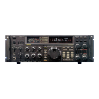
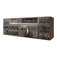
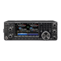
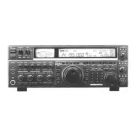
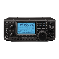
• MAIN CPU (LOGIC UNIT: IC604)
for
free
by
RadioAmateur.eu