4 - 7
AMP
PLL
IC
BUFF
FIL
LOOP
BUFF
VCO
SW
BUFF
VCO
SW
Q73
D91
Q76
Q74
D160
Q62
D87
Q61
D86
D92
IC14
D89
Q72
TCXO
15.3MHz
R_PLLSTB
PLLDATA
PLLCK
X1
Q60
IC45
D102
D90
164.350
−
220.350 MHz
353.65
−
523.170 MHz
To the TX amplifiers
or
LO filters
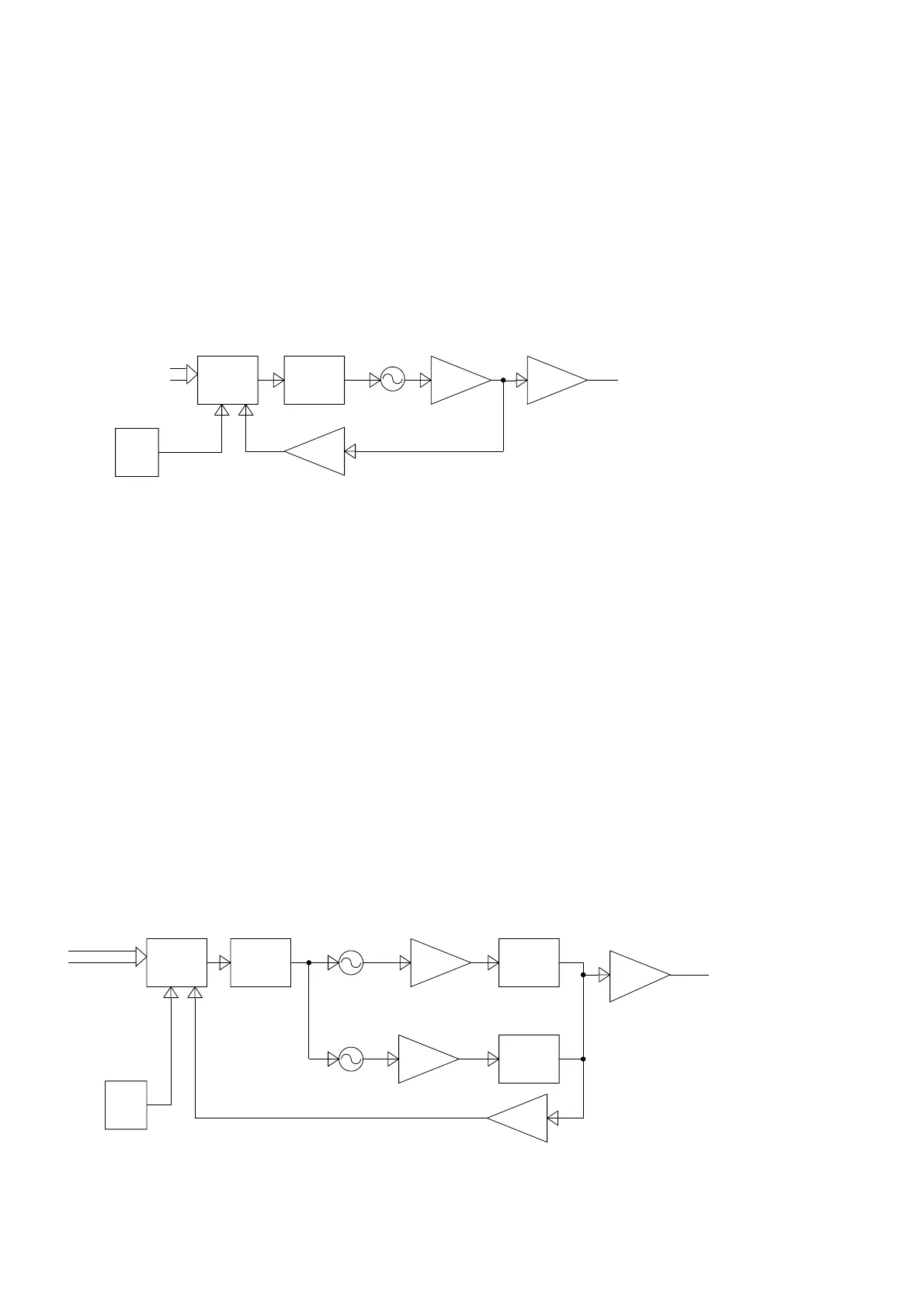
PLL CIRCUITS
The PLL circuit provides stable oscillation of the transmit
frequency and receive 1st LO frequency. The PLL output
frequency is controlled by the divided ratio (N-data) from the
CPU.
LEFT BAND VCO LOOP
A portion of VCO output signals from the buffer (Q113)
are applied to the PLL IC (IC41) via another buffer (Q112).
The applied signals are
divided at the prescaler and
programmable counter according to the control signals
(“L_PLLSTB,” “PLLDATA” and "PLLCK”) from the CPU.
The divided signal is phase-compared with the 12. 8 MHz
reference frequency signal from the reference frequency
oscillator (X5), at the phase detector.
PLLCK
PLLDATA
L_PLLSTB
BUFF
FIL
LOOP
AMP
PLL
IC
BUFF
IC44
12.8MHz
D145
Q111
Q113
TCXO
X5
Q112
D146
D147
135.575 −255.575 MHz
To the TX amplifiers
or
LO filters
IC41
The phase difference is output from pin 5 as a pulse type
signal after being passed through the internal charge pump.
The output signal is converted into the DC voltage (lock
voltage) by passing through the loop filter (R694, 696–
698, C760–762). The lock voltage is applied to the variable
capacitors (D145 and D146), and locked to keep the VCO
frequency constant.
If the oscillated signal drifts, its phase changes from that of
the reference frequency, causing a lock voltage change to
compensate for the drift in the VCO oscillating frequency.
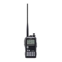
RIGHT BAND RX VCO LOOP
A portion of VCO output signals from the buffer (Q74) are
applied to the PLL IC (IC14) via the VCO switch (D160) and
another buffer (Q112). The applied signals are
divided at
the prescaler and programmable counter according to the
control signals (“R_PLLSTB,” “PLLDATA” and "PLLCK”) from
the CPU. The divided signal is phase-compared with the 15.3
MHz reference frequency signal from the reference frequency
oscillator (X1), at the phase detector.
The phase difference is output from pin 5 as a pulse type
signal after being passed through the internal charge pump.
The output signal is converted into the DC voltage (lock
voltage) by passing through the loop filter (Q61, 62, D86).
The lock voltage is applied to the variable capacitors (D91,
92), and locked to keep the VCO frequency constant.
RIGHT BAND TX/RX VCO
A portion of VCO output signals from the buffer (Q76) are
applied to the PLL IC (IC14) via the VCO switch (D102)
and another buffer (Q60). The applied signals are
divided
at the prescaler and programmable counter according to the
control signals (“R_PLLSTB,” “PLLDATA” and "PLLCK”) from
the CPU. The divided signal is phase-compared with the 15.3
MHz reference frequency signal from the reference frequency
oscillator (X1), at the phase detector.
The phase difference is output from pin 5 as a pulse type
signal after being passed through the internal charge pump.
The output signal is converted into the DC voltage (lock
voltage) by passing through the loop filter (Q61, 62, D86).
The lock voltage is applied to the variable capacitors (D91,
92), and locked to keep the VCO frequency constant.
•
LEFT BAND VCO LOOP
•
RIGHT BAND RX AND TX/RX VCO LOOP