4-2-2 MODULATION CIRCUITS
The modulation circuit modulates the VCO oscillating signal
(RF signal) using the audio signals from the microphone.
The AF signals from the D/A converter (IC8, pin 3) change
the reactance of varactor diode (D18) to modulate the oscil-
lated signal at the TX VCO circuit (Q13, D17, D21). The
modulated VCO signal is amplified at the buffer amplifiers
(Q10, Q12) and then applied to the drive amplifier circuit via
the T/R switch (D14).
The CTCSS/DTCS signals (“CENC0,” “CENC1,” “CENC2”)
from the CPU (IC13, pins 23–25) pass through the low-pass
filter (IC5, pins 12 and 14) via 3 registers (R191–R193) to
change its waveform. Then the signals are applied to the
D/A converter (IC8, pin 9). The output signals from the D/A
converter (IC8, pin 10) pass through the low-pass filter
(IC6, pins 6 and 7) to be mixed with “MOD” signal, and then
applied to the D/A converter again (IC8, pin 4) after passing
through the analog switch (IC10, pins 8 and 9).
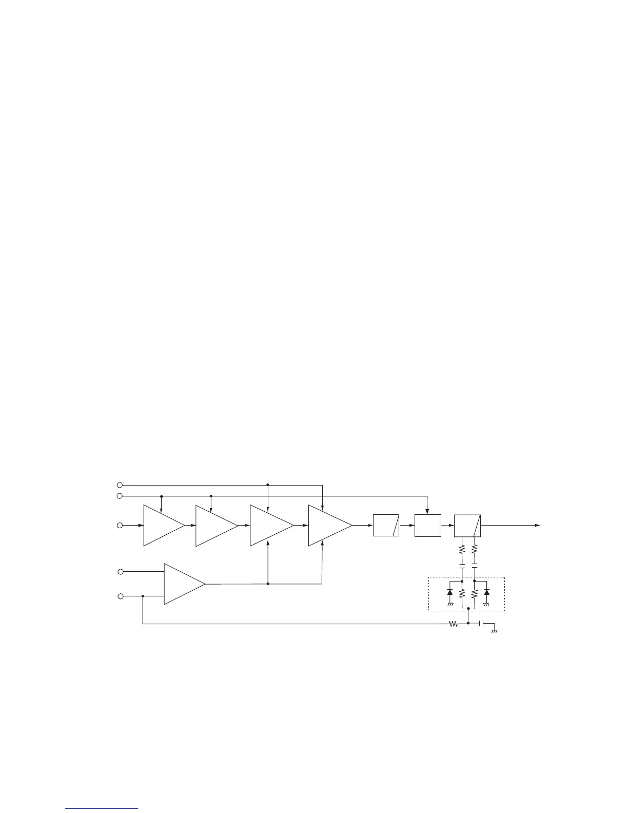
4-2-3 TRANSMIT AMPLIFIER CIRCUITS
Transmit amplifiers amplify the TX VCO oscillating signal to
transmit power level.
The modulated RF signal from the TX VCO circuit passes
through the T/R switch (D14) and is amplified at the YGR
(Q9), pre-drive (Q5), drive (Q8), and power (Q7) amplifiers
to obtain 4 W (max.) of RF power (at 7.2 V DC).
The amplified signal passes through the low-pass filter (L4,
C11, C13, C16), antenna switch (D2), the low-pass filter (L1
–L3, C2–C5, C175, C176) and power detector (D1, D30),
then applied to the antenna connector (CHASSIS unit; J1).
4-2-4 APC CIRCUITS
The bias current of the drive (Q8) and power (Q7) amplifiers
are controlled by the APC circuit.
The APC circuit (IC2, D1, D30) protects drive and power
amplifiers from the reflected signal, and selects output
power of HIGH, LOW2 or LOW1.
The power detector (D1, D30) detects transmit output power
and converts it into DC voltage. The DC voltage is at a mini-
mum level when the antenna impedance is matched to 50
Ω,
and increased when mismatched.
The detected voltage is applied to the differential amplifier
(IC2, pin 3), and the “T2” signal from the D/A converter (IC8,
pin 23), controlled by the CPU (IC13), is applied to pin 1 for
reference. When antenna impedance is mismatched, the
detected voltage exceeds the power setting voltage. Then
the output voltage of the differential amplifier (IC2, pin 4)
controls the input current of the drive (Q8), and power (Q7)
amplifiers to reduce the output power.
4 - 3
Power
AMP
APC
AMP
Drive
AMP
+
–
VCC
to ANT
T2
TMUT
RF signal
from Buffer AMP
T5V
D30 D1
YGR
AMP
ANT
SW
LPF
LPF
Q5
IC2
Q9
Q8
Q7
D2, D5
Power DET
Pre-drive
AMP
• APC CIRCUITS
 Loading...