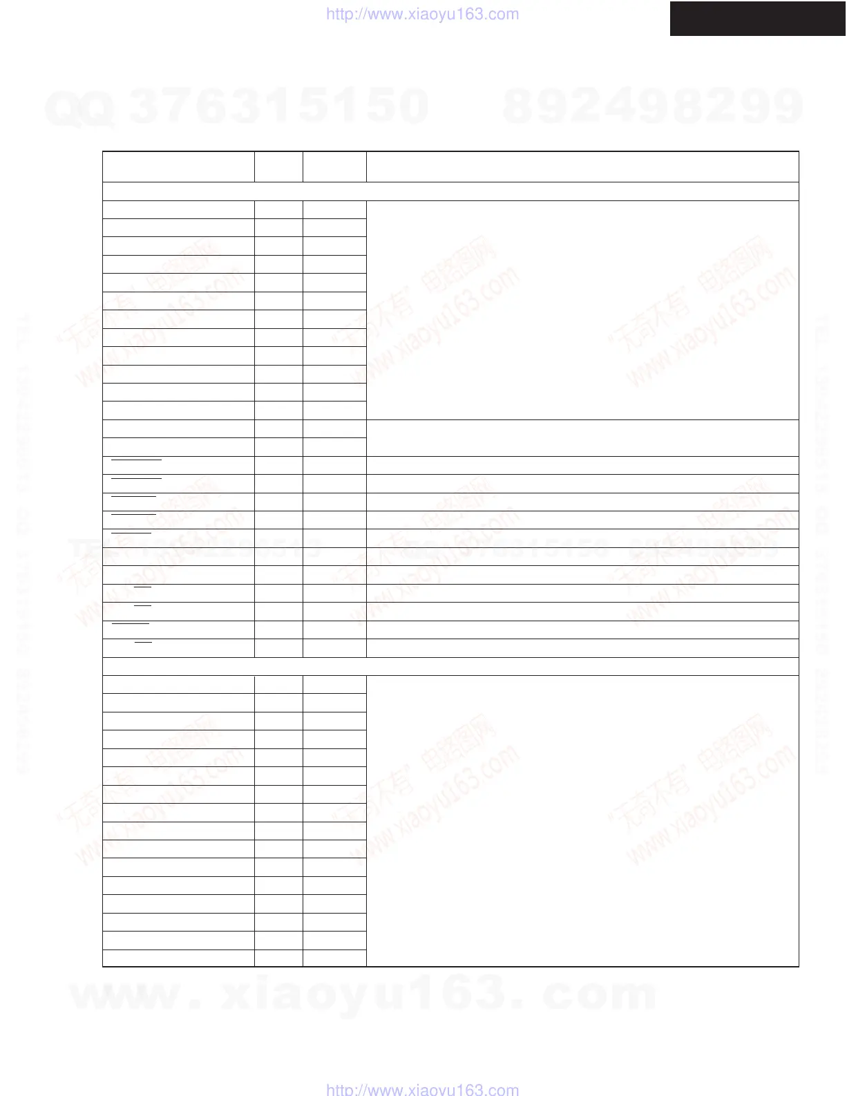
IC BLOCK DIAGRAMS AND TERMINAL DESCRIPTIONS -29
Q3601 : D707E001BRFP250 (32 bit Floating-Point Digital Signal Processor)
TERMINAL DESCRIPTION(1/3)
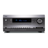
TX-SR876/SA876
TYPE
External Memory Interface (EMIF) Addressand Control
EM_A[0] 91 O
EM_A[1] 89 O
EM_A[2] 88 O
EM_A[3] 86 O
EM_A[4] 84 O
EM_A[5] 83 O
EMIF Address Bus
EM_A[6] 80 O
EM_A[7] 79 O
EM_A[8] 76 O
EM_A[9] 75 O
EM_A[10] 93 O
EM_A[11] 74 O
EM_BA[0] 96 O
SDRAM Bank Address and Asynchronous Memory
Low-Order Address
EM_BA[1] 94 O
EM_CS[0]
97 O SDRAM Chip Select
EM_CS[2] 100 O Asynchronous Memory Chip Select
EM_CAS 37 O SDRAM Column Address Strobe
EM_RAS 98 O SDRAM Row Address Strobe
EM_WE 38 O SDRAM Write Enable
EM_CKE 71 O SDRAM Clock Enable
EM_CLK 70 O SDRAM Clock
EM_WE_DQM[0] 39 O Write Enable or Byte Enable for EM_D[7:0]
EM_WE_DQM[1] 67 O Write Enable or Byte Enable for EM_D[15:8]
EM_OE 104 O SDRAM Output Enable
EM_RW 102 O Asynchronous Memory Read/not Write
SIGNAL NAME PIN NO. DESCRIPTION
External Memory Interface (EMIF) Data Bus
EM_D[0] 52 IO
EM_D[1] 51 IO
EM_D[2] 49 IO
EM_D[3] 48 IO
EM_D[4] 46 IO
EM_D[5] 45 IO
EM_D[6] 43 IO
EM_D[7] 41 IO
EM_D[8] 66 IO
EM_D[9] 64 IO
EM_D[10] 63 IO
EM_D[11] 61 IO
EM_D[12] 59 IO
EM_D[13] 58 IO
EM_D[14] 56 IO
EM_D[15] 55 IO
EMIF Data Bus [Lower 16 Bits]
w
w
w
.
x
i
a
o
y
u
1
6
3
.
c
o
m
Q
Q
3
7
6
3
1
5
1
5
0
9
9
2
8
9
4
2
9
8
T
E
L
1
3
9
4
2
2
9
6
5
1
3
9
9
2
8
9
4
2
9
8
0
5
1
5
1
3
6
7
3
Q
Q
TEL 13942296513 QQ 376315150 892498299
TEL 13942296513 QQ 376315150 892498299
http://www.xiaoyu163.com
http://www.xiaoyu163.com
 Loading...