OVERVIEW OF NUMERIC PROCESSING
As
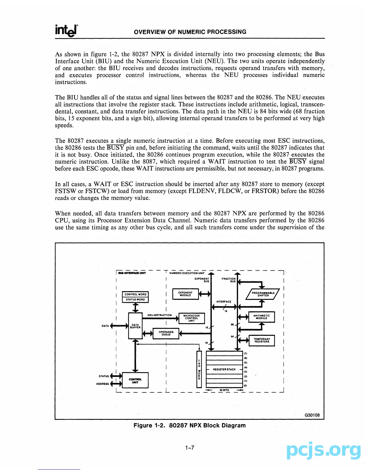
shown
in
figure
1-2,
the 80287 NPX
is
divided internally into
two
processing elements; the
Bus
Interface Unit (BIU) and the Numeric Execution Unit (NEU). The
two
units operate independently
of one another: the BIU receives and decodes instructions, requests operand transfers with memory,
and executes processor control instructions, whereas the
NEU
processes individual numeric
instructions.
The
BIU handles all of the status and signal lines between the
80287
and the 80286. The NEU executes
all instructions that involve the register stack. These instructions include arithmetic, logical, transcen-
dental, constant, and data transfer instructions. The data path in the
NEU
is
84
bits
wide
(68 fraction
bits, 15 exponent bits, and a sign bit), allowing internal operand transfers to be performed at very high
speeds.
The 80287 executes a single numeric instruction at· a time. Before executing most ESC instructions,
the 80286 tests the BUSY pin and, before initiating the command, waits until the 80287 indicates that
it
is
not busy. Once initiated, the 80286 continues program execution, while the 80287 executes the
numeric instruction. Unlike the 8087, which required
aWAIT
instruction to test the BUSY signal
before each ESC opcode, these WAIT instructions are permissible, but not necessary,
in
80287
programs.
In all cases, a WAIT or ESC instruction should
be
inserted after any 80287 store
to
memory (except
FSTSW or FSTCW)or load from memory (except FLDENV, FLDCW, or FRSTOR) before the 80286
reads or changes the memory value.
When needed, all data transfers between memory and the 80287
NPX
are performed
by
the 80286
CPU, using its Processor Extension Data Channel. Numeric data transfers performed
by
the 80286
use the same timing as any other bus cycle, and all such transfers come under the supervision of the
DATA
STATUS
ADDRESS
OPERANDS
QUEUE
MICROCODE
CONTROL
UNOT
T
•
G
w
o
•
o
II
I-
III
1-----;'51
REGISTER
STACK
_____
L
_____
...!!II!!.
____
.J
Figure 1-2.
80287
NPX Block Diagram
1-7
G30108