Intel
®
5100 MCH Chipset
Intel
®
5100 Memory Controller Hub Chipset for Communications, Embedded, and Storage Applications
TDG July 2008
10 Order Number: 318676-003US
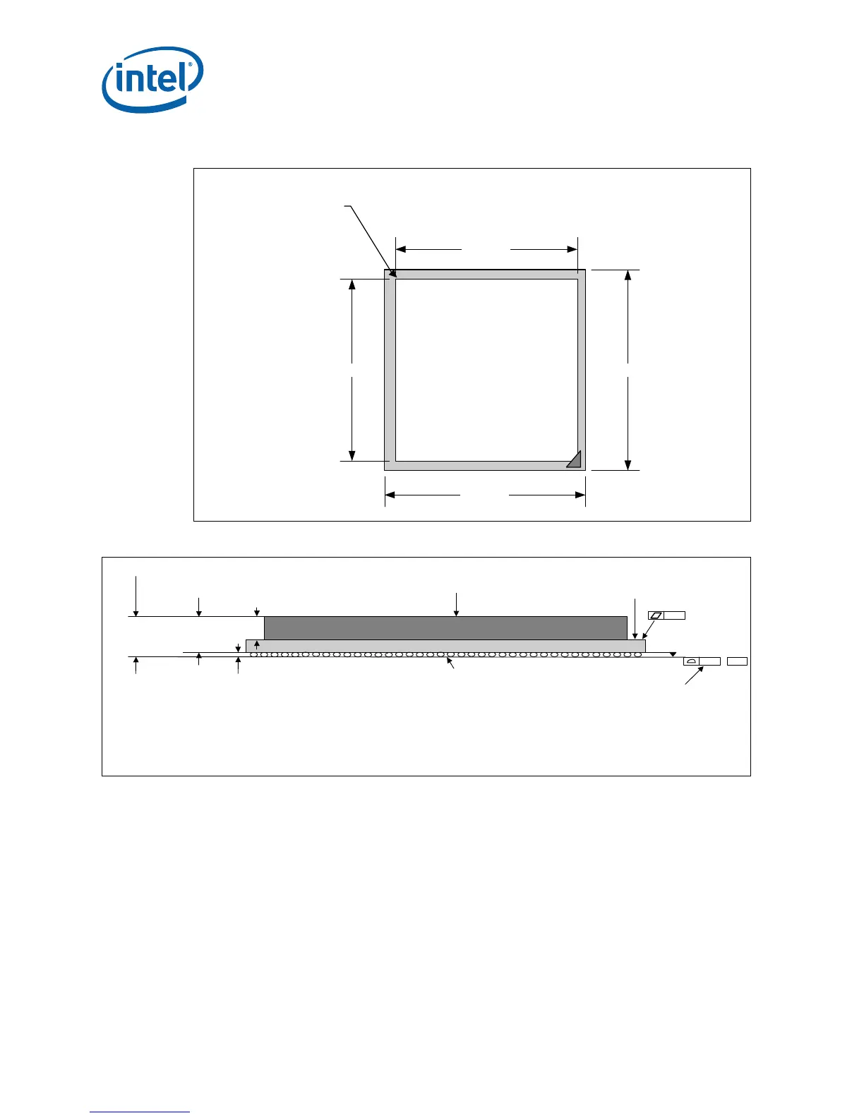
Figure 2. MCH Package Dimensions (Top View)
Figure 3. MCH Package Dimensions (Side View)
MCH
IHS
Handling
Exclusion
Area
42.5 mm.
42.5 mm.38.5 mm.
38.5 mm,
0.20
–C–
IHS
Substrate
0.435 ± 0.025 mm
See note 3
Seating Plane
2.44 ± 0.071 mm
See note 1.
Notes:
1. Primary datum -C- and seating plan are defined by the spherical crowns of the solder balls (shown before motherboard attach)
2. All dimensions and tolerances conform to ANSI Y14.5M-1994
3. BGA has a pre-SMT height of 0.5mm and post-SMT height of 0.41-0.46mm
4. Shown before motherboard attach; FCBGA has a convex (dome shaped) orientation before reflow and is expected to have a slightly concave (bowl shaped)
orientation after reflow
0.20
See note 4.
3.79 ± 0.144 mm
4.23 ± 0.146 mm
 Loading...