© 2020 Jackson Labs Technologies, Inc. 19
LTE-Lite User Manual
The synthesized frequency is generated by a PLL circuit inside the microprocessor, and uses a VCO
to generate the reference frequency. Due to the nature of the VCO/PLL circuit the phase noise and
spurs of this output are higher than the TCXO-generated RF output. The output frequency will be
phase-locked to the TCXO frequency, and thus to UTC(GPS). Due to the synthesizer being
software-controlled, the synthesized output will take up to 1 second typically to appear on the output
pin. An external PHASE-LOCK indicator pin 7 on the module indicates when the synthesized output
frequency is stable, and this output signal can be used by external circuitry as a generic CMOS
RESET# signal.
Frequency selection is done by three internally-pulled-up strap pins on the module (pins 25, 26 and
27) and leaving these pins unconnected causes the synthesized output to be disabled for lower power
consumption and reduced EMI noise.
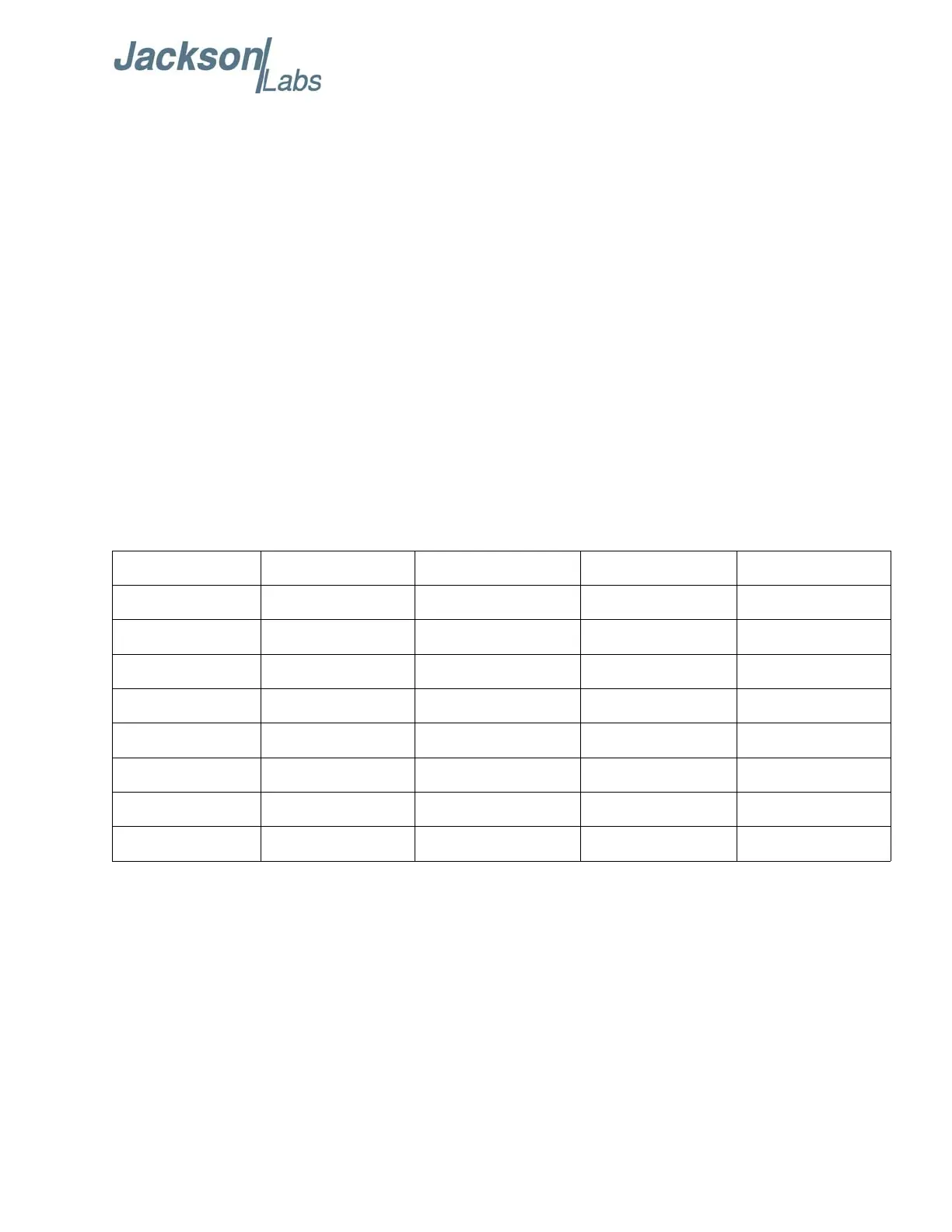
The synthesized output frequencies depend on the TCXO frequency that is used on the module.
Table 2.2 shows the available output frequency selections based on the TCXO frequency and the
required resistor straps for the desired synthesized frequency. Leaving an FS strap pin unconnected
results in a 1 (high) state, and pulling it to ground results in a 0 (low) state.
2.3.9 System Reset
The LTE-Lite SMT Module contains internal reset circuitry and thus does not require an external
reset input. Pin 23 of the module is an open-collector reset input that can be pulled to ground to
initiate a manual system reset of the module. This pin is typically left un-connected, or it can be
connected to a reset switch. Initiating a system reset will cause the GPS receiver to not generate GPS
fixes for up to 35 seconds if power had been off for prolonged periods of time, and down to 3 seconds
typically if the unit had been powered-on recently.
Table 2.2 Synthesized Output Frequency versus Resistor Straps and TCXO
Frequency
FS2/FS1/FS0 10 MHz TCXO 15.36 MHz TCXO 19.2 MHz TCXO 20 MHz TCXO
111 disabled disabled disabled disabled
110 5MHz 4.608MHz 4.8MHz 5MHz
101 13.33333333MHz 10.24MHz 9.6MHz 10MHz
100 16MHz 15.36MHz 12.8MHz 13.33333333MHz
011 20MHz 23.04MHz 15.36MHz 16MHz
010 26.66666667MHz 30.72MHz 25.6MHz 26.66666667MHz
001 40MHz 46.08MHz 38.4MHz 40MHz
000 80MHz 92.16MHz 76.8MHz 80MHz