20
HIGH FREQUENCY PROCESSING
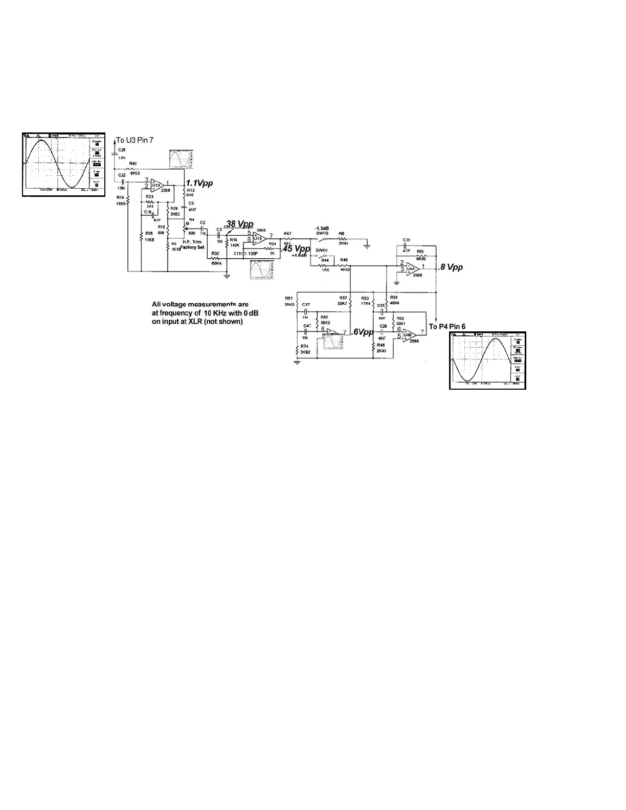
The circuit, shown above, is used for the high frequency processing of the input signal.
Physically, it is located on the input circuit board. Its purpose is to actively filter out or attenuate
the low frequency component from the composite signal leaving only the high frequencies to be
contoured by the user and, eventually, sent to power amplifier for final amplification.
Specifically, signal from the previous stage enters the non-inverting input pin 3 of
integrated circuit U1A through coupling capacitor C26. U1A, acting as a second order high pass
filter, attenuates signals below the critical frequency, according to the equation:
f(c) = 1/[2π(R1R2C1C2)1/2] = where R1 = 9kΩ, R2 = 10kΩ, C1 = C2 = 10nF
= 1.677kHz
Because of this relationship, the frequency response will “roll-off” or be attenuated at a
rate of –40 dB per decade assuring a gain of .707 volts at this critical frequency.
Integrated circuit U1B is configured as a buffer amplifier to isolate the effects of the user
selectable high frequency “trim” potentiometer, R4, and includes some additional second-order
filtering. Partial equalization occurs from components R13 and C5. The signal enters at pin 5
and pin 6 of this IC whereby unwanted noise is eliminated through CMRR, and it is amplified
from a signal voltage of .38V to a usable voltage level of .45 volts. The signal exits at pin 7.
Enabling of SW1G and SW1H cause signal frequency equalization boosts or cuts to occur.
These can be attributed to the effects of U4A and B along with U8.
Out
ut= . 8 V
In
ut= 1 V