UNCLASSIFIED 10/27/2021
` UNCLASSIFIED ii
TABLE OF CONTENTS
1 Introduction................................................................................................................ 1
1.1 Purpose ............................................................................................................... 1
1.2 Scope................................................................................................................... 1
2 Equipment Overview................................................................................................ 1
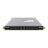
2.1 Identification of Chassis.................................................................................... 1
2.2 Description of Field Replaceable Units (FRU) .............................................. 2
3 Power Down and Removal of Non-Volatile Storage ........................................... 2
3.1 System Power Down......................................................................................... 2
3.2 Disassembly of the QFX5120-48Y Chassis and Identification of NV
storage ........................................................................................................................... 2
3.3 Remove Non-volatile components from the System Board ...................... 13
3.4 Follow the assembly procedure in reverse order to assemble the
QFX5120-48Y Chassis.............................................................................................. 13
TABLE OF FIGURES
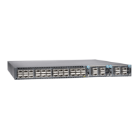
Figure 1 QFX5120-48Y Front view................................................................................ 2
Figure 2 QFX5120-48Y PSU FRUs and FAN FRUs .................................................. 3
Figure 3 Top cover screws – Top view ......................................................................... 3
Figure 4 Screws on left and right side of the system.................................................. 4
Figure 5 Top cover screws on bottom side. ................................................................. 4
Figure 6 Slide & lift the top Cover .................................................................................. 5
Figure 7 Locating and removing main board ............................................................... 6
Figure 8 Locating main board heatsink support plate ................................................ 7
Figure 9 Main board heatsink support plate removed ................................................ 7
Figure 10 Main board SPI device for CPLD and FPGA ............................................. 8
Figure 11 Main board IDEEPROM ................................................................................ 8
Figure 12 Main board QSPI device ............................................................................... 9
Figure 13 CPU Board volatile and non-volatile memory devices ........................... 10
Figure 14 M.2 SATA SSD device on CPU Board. .................................................... 11
Figure 15 BIOS devices on CPU Board. .................................................................... 12
Figure 16 Management EEPROM on CPU Board. ................................................... 12
Figure 17 CPU board IDEEPROM and CPLD SPI Flash ........................................ 13