INDEX
INDEX-1
SECTION 1 OUTLINE OF THE PROCUCTS
1.1 COMPARSION TABLE OF DV MODELS SPECIFICATION BY PRODUCTS YEAR.............1-1
1.1.1 Comparison table of DV models specification by products year.....................................1-1
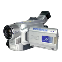
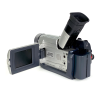
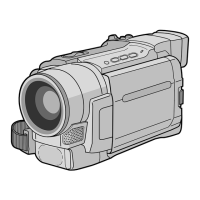
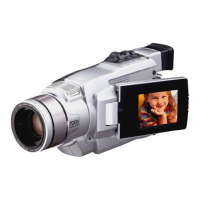
1.1.2 Specification of the DVC models....................................................................................1-3
SECTION 2 EXPLANATION OF ELECTRICAL CIRCUIT
2.1 CIRCUIT OUTLINE ..............................................................................................................2-1
2.1.1 Basic block diagram.......................................................................................................2-1
2.2 CCD (ICX220AK/ICX221BK)................................................................................................2-2
2.2.2 CCD Image Sensor........................................................................................................2-3
2.2.3 Numbers of pixel for main models..................................................................................2-6
2.3 EXPLANATION OF CAMERA CIRCUIT ...............................................................................2-7
2.3.1 Present AW / AE control system ....................................................................................2-7
2.3.2 AF (Auto Focus) control.................................................................................................2-13
2.3.3 EIS (Electric Image Stabilizer) control............................................................................2-14
2.4 CAMERA SYSREM IC'S FUNCTION...................................................................................2-15
2.4.1 Camera DSP (IC4301: JCY0120) function.....................................................................2-15
2.5 EXPLANATION OF DECK CIRCUIT ....................................................................................2-22
2.5.1 Deck system overall structure........................................................................................2-22
2.5.2 PB equalizer and ATF....................................................................................................2-23
2.5.3 PLL operation ................................................................................................................2-24
2.5.4 Basic principle of Viterbi detection .................................................................................2-25
2.5.5 Audio recording mode....................................................................................................2-26
2.5.6 Audio signal processing.................................................................................................2-27
2.5.7 Clock system for audio data...........................................................................................2-28
2.5.8 Deck DSP IC function....................................................................................................2-29
2.5.9 Audio AMP IC function...................................................................................................2-35
2.6 SYSCON CPU .....................................................................................................................2-38
2.6.1 Contents of SYSCON CPU processing..........................................................................2-38
2.6.3 System composition.......................................................................................................2-39
2.6.4 SYSCON CPU block diagram........................................................................................2-40
2.6.5 SYSCON CPU (IC1001: MN1021617HL) pin functions..................................................2-41
2.7 DECK CPU...........................................................................................................................2-44
2.7.1 Contents of DECK CPU processing...............................................................................2-44
2.7.2 DECK system composition.............................................................................................2-44
2.7.3 Tracking Error information..............................................................................................2-45
2.7.4 1394 interface control ....................................................................................................2-46
2.7.5 JLIP Video Capture........................................................................................................2-46
2.7.6 DECK CPU block diagram .............................................................................................2-47
2.7.7 Deck CPU (IC1401: MN103004KRH) pin functions........................................................2-48