5
4
3
2
1
A
BC
DE
F
G
2-15 2-16
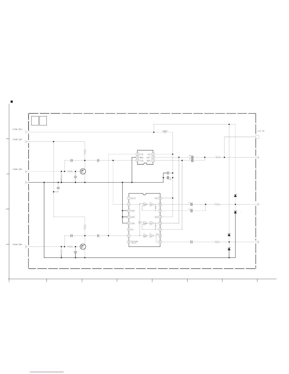
MAIN(V-OUT)
SCHEMATIC DIAGRAM
D4702
Q4702
D4701
D4703
C4714
D4704
CN25
R4707
R4701
SY_OUT
V_OUT
SC_OUT
C4706
R4703
R4709
C4716
C4703
C4717
R4710
IC4702
C4707
C4715
REG_4.8V
C4701
GND
CAM_Y
CAM_C
Q4701
IC4701
C4704C4702
R4704
C4713
C4705
DAC_3.2V
L4701
C4709
R4712
R4706
R4713
C4708
2SA1774
#
V_OUT
/4
/6.3
#
2SA1774
#
/6.3V
#
#
T
240
240
100
680
680
27p
5p
5p
1.2K
22
127p
1.2k
0.01
22µ
10
68
0.1
MM1512XN-X
BA7665FS-X
0 1
MAIN(V-OUT)
y30257001a_rev0.1
NOTES : 1. The parts with marked() is not used.
2. For V-OUT waveforms,please refer to page 2-43.
NOTES : ٨For the destination of each signal and further line connections that are cut off from this diagram,
refer to "BOARD INTERCONNECTIONS".
٨When ordering parts, be sure to order according to the Part Number indicated in the Parts List.
17