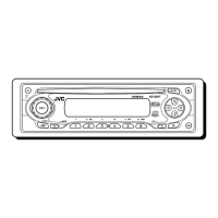
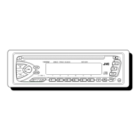
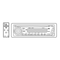
KD-S890
(No.49799)1-27
SECTION 4
Description of major ICs
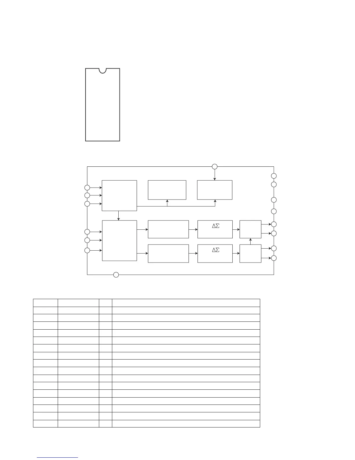
4.1 AK4381VT-X (IC481) : D/A converter
•Pin layout
• Block diagram
• Pin functions
MCLK
BICK
SDTI
LRCK
PDN
CSN
CCLK
CDTI
DZFL
DZFR
VDD
VSS
AOUTL+
AOUTL-
AOUTR+
AOUTR-
1
2
3
4
5
6
7
8
16
15
14
13
12
11
10
9
Pin No. Symbol I/O Description
1 MCLK I Master clock input terminal
2 BICK I Audio serial data clock terminal
3 SDTI I Audio serial data input terminal
4 LRCK I L/R Clock terminal
5 PDN I Power down mode terminal
6 CSN I Chip select
7 CCLK I Control data input terminal
8 CDTI I Control data input terminal
9 AOUTR- O Rch negative analog output terminal
10 AOUTR+ O Rch positive analog output terminal
11 AOUTL- O Lch negative analog output terminal
12 AOUTL+ O Lch positive analog output terminal
13 VSS - Connect to ground
14 VDD - Power supply terminal
15 DZFR O Rch data zero input detection terminal
16 DZFL O Lch data zero input detection terminal
De-emphasis
Control
8X
Interpolator
uP
Interface
Audio
Data
Interface
CSN
CCLK
CDTI
LRCK
BICK
SDTI
PDN
8X
Interpolator
Modulator
SCF
SCF
Clock
Divider
VDD
VSS
DZFL
DZFR
MCLK
AOUTL+
AOUTR+
AOUTR-
AOUTL-
Modulator
 Loading...