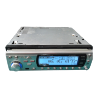
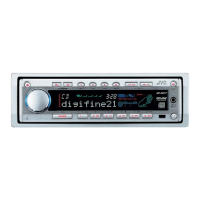
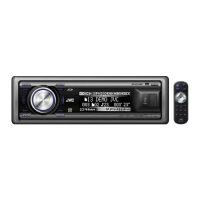
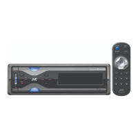
1-38 (No.49841)
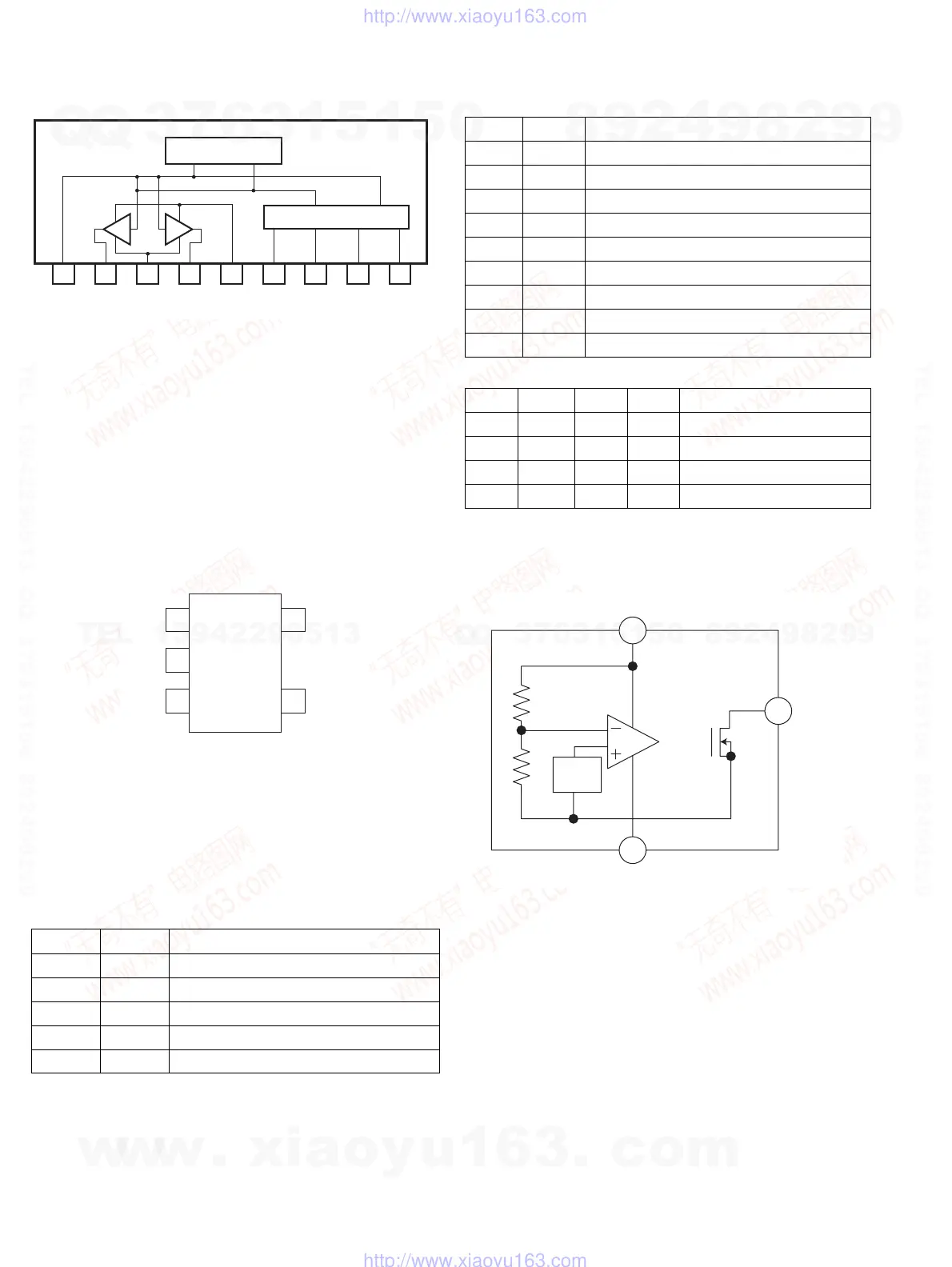
4.3 BA6956AN (IC981) : Reversible motor driver
• Pin layout & Block diagram • Pin function
• Truth table
4.4 BD4833FVE-W (IC702) : Regulator
• Pin layout • Block diagram
• Pin functions
TSD
CONTROL LOGIC
1 2 3 4 5 6 7 8 9
VREF
OUT2
RNF
OUT1
VM
Vcc
FIN
GND
RIN
Pin No. Symbol Function
1 VREF Output high voltage level control terminal
2 OUT2 Output terminal for motor
3 RNF GND of driver division
4 OUT1 Output terminal for motor
5 VM Power supply for driver division
6 Vcc Power supply for signal division
7 FIN Input terminal for control logic
8GNDGND
9 RIN Input terminal for control logic
FIN RIN OUT1 OUT2 MODE
H L H L Forward rotation mode
L H L H Reverse rotation mode
H H L L Break Mode
L L OPEN OPEN Stand-by mode
VOUT
SUB
N.C.
1
2
3
5
4
VDD
GND
VOUT
GND
VDD
Vref
Pin No Symbol Function
1 VOUT Reset output
2 SUB Sub slate (connect to GND)
3 N.C. Non connect
4GNDGND
5 VDD Power supply voltage
w
w
w
.
x
i
a
o
y
u
1
6
3
.
c
o
m
Q
Q
3
7
6
3
1
5
1
5
0
9
9
2
8
9
4
2
9
8
T
E
L
1
3
9
4
2
2
9
6
5
1
3
9
9
2
8
9
4
2
9
8
0
5
1
5
1
3
6
7
3
Q
Q
TEL 13942296513 QQ 376315150 892498299
TEL 13942296513 QQ 376315150 892498299
http://www.xiaoyu163.com
http://www.xiaoyu163.com

 Loading...