(No.49841)1-39
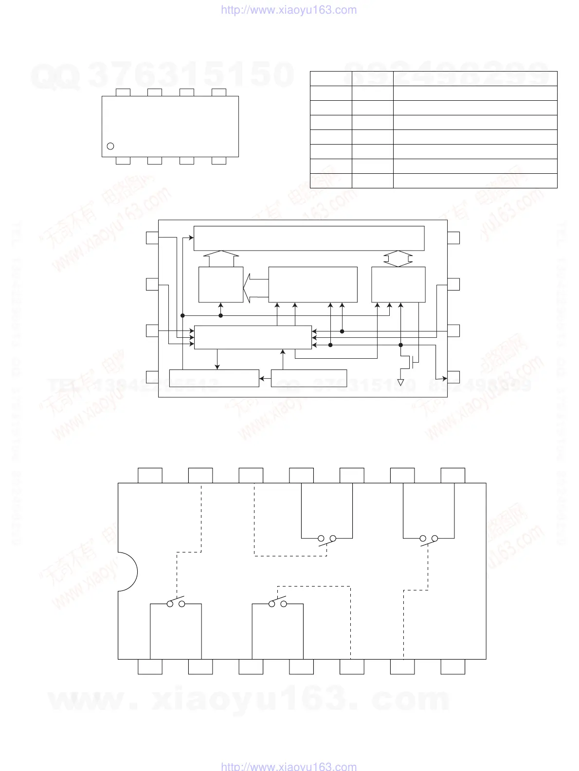
4.5 BR24L32F-W-X (IC703) : EEPROM
• Pin layout • Block diagram
• Block diagram
4.6 BU4066BCFV-X (IC322,IC351) : Quad analog switch
• Pin layout & Block diagram
Vcc WP SCL SDA
A0 A1 A2 GND
Symbol I/O Function
A0A1A2 I Slave address set
GND - Ground (0V)
SDA I/O Slave and word address
Serial data input serial data output
SCL I Serial clock input
WP I Write protect input
VCC - Power supply
8 Vcc
7 WP
6 SCL
5 SD
A0 1
A1 2
A2 3
GND 4
32kbit EEPROM array
12bits
12bits
8bits
Address
decoder
Slave word
address register
Data
register
START
STOP
ACK
Control logic
High voltage generator Vcc level detect
14 13 12 11 810 9
1234 756
VDD C1 C4 I/O4 I/O3O/I4 O/I3
I/O1 O/I1 O/I2 I/O2 VssC2 C3
w
w
w
.
x
i
a
o
y
u
1
6
3
.
c
o
m
Q
Q
3
7
6
3
1
5
1
5
0
9
9
2
8
9
4
2
9
8
T
E
L
1
3
9
4
2
2
9
6
5
1
3
9
9
2
8
9
4
2
9
8
0
5
1
5
1
3
6
7
3
Q
Q
TEL 13942296513 QQ 376315150 892498299
TEL 13942296513 QQ 376315150 892498299
http://www.xiaoyu163.com
http://www.xiaoyu163.com
 Loading...