KS-FX742R
1-26 (No.49816)
4.6 SAA6579T-X(IC71):RDS detecter
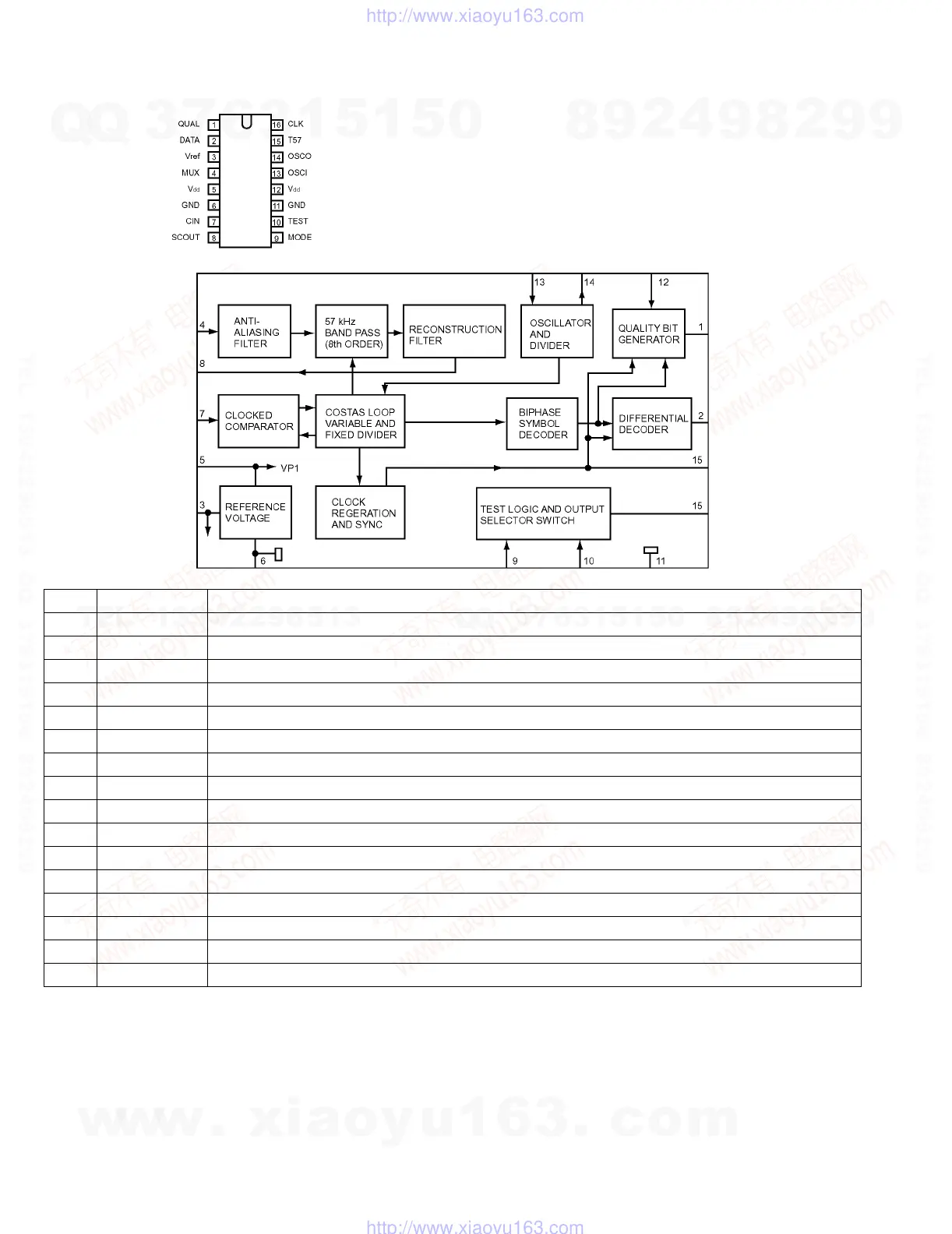
• Pin layout
• Block diagram
• Pin function
Pin No. Symbol Description
1 QUAL Quality indication output
2 DATA RDS data output
3 Vref Reference voltage output (0.5VDDA)
4 MUX Multiolex signal input
5 Vdd +5V supply voltage for analog part
6 GND Ground for analog part (0V)
7 CIN Sub carrier input to comparator
8 SCOUT Sub carrier output of reconstruction filter
9 MODE Oscillator mode / test control input
10 TEST Test enable input
11 GND Ground for digital part (0V)
12 Vdd +5V supply voltage for digital part
13 OSCI Oscillator input
14 OSCO Oscillator output
15 T57 57 kHz clock signal output
16 CLK RDS clock output
w
w
w
.
x
i
a
o
y
u
1
6
3
.
c
o
m
Q
Q
3
7
6
3
1
5
1
5
0
9
9
2
8
9
4
2
9
8
T
E
L
1
3
9
4
2
2
9
6
5
1
3
9
9
2
8
9
4
2
9
8
0
5
1
5
1
3
6
7
3
Q
Q
TEL 13942296513 QQ 376315150 892498299
TEL 13942296513 QQ 376315150 892498299
http://www.xiaoyu163.com
http://www.xiaoyu163.com
 Loading...