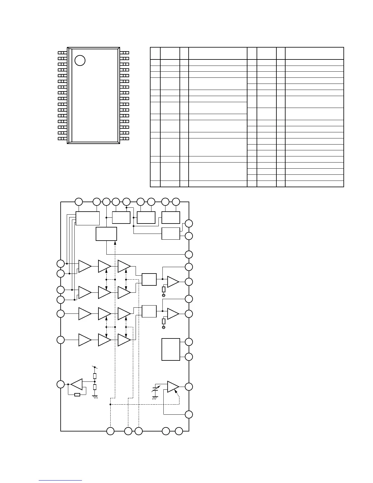
MX-KA3
1-27
AN22000A (IC611) : CD-DA Head Amp.
1. Terminal layout
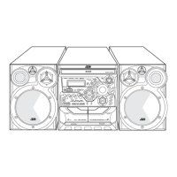
3. Block diagram
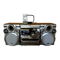
2. Pin function
1
16 17
RF_EQ
NRFDET
AMP
AGC
6
24
754 8
BDO
SUBT
11 12
OFTR
3TENV
VDET
13 14
9
10
15
32
31
22
23
GCA BCA
AMP
30
29
GCA BCA
+
-
AMP
SUBT
27
28
21
20
19
18
GCA BCA
AMP
17
GCA BCA
+
-
2
1
+
-
-
+
RFOUT
RFIN
GCTL
26
TBAL
25 16 3
FBAL
LD
PD
Pin
No.
Function
Symbol
I/O
Pin
No.
Function
Symbol
I/O
1 PD I APC Amp. input terminal
2 LD O APC Amp. output terminal
3 VCC - Power supply terminal
4 RFN I RF adder Amp. inverting input
terminal
5 RFOUT O RF adder Amp. output terminal
6 RFIN I AGC input terminal
7 CAGC I Input terminal for AGC loop
filter capacitor
8 ARF O AGC output terminal
9 CBA I Capacitor connecting terminal
for HPF-Amp.
10 3TOUT O 3 TENV output terminal
11 CBOO I Capacitor connecting terminal
for envelope detection on the
darkness side
12 BDO O BDO output terminal
13 COFTR I Capacitor connecting terminal
for envelope detection on the
light side
14 OFTR O OFTR output terminal
15 NRFDET O NRFDET output terminal
16 GND - Ground
17 VREF O VREF output terminal
18 VDET O VDET output terminal
19 TEBPF I VDET output terminal
20 TEOUT O TE Amp. output terminal
21 TEN I TE Amp. inverting input
terminal
22 FEN I FE Amp. inverting input
terminal
23 FEOUT O FE Amp. output terminal
24 GCTL O GCTL & APC terminal
25 FBAL O FBAL control terminal
26 TBAL O TBAL control terminal
27 E I Tracking signal input terminal 1
28 F I Tracking signal input terminal 2
29 D I Focus signal input terminal 4
30 B I Focus signal input terminal 3
31 C I Focus signal input terminal 2
32 A I Focus signal input terminal 1
23