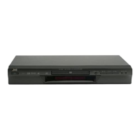
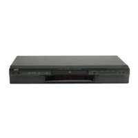
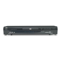
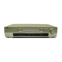
XV-S300BK/XV-S332SL/XV-S402SL/XV-S403SG
30
4.6.3 Pin function
4.7 74VHCT08ASJ-X (IC704) : 2-input AND gate
4.7.1 Pin layout 4.7.2 Truth table
Pin No. Symbol I/O Description
1 NC - Non connect
2 A3 O Output 3 for spindle motor
3 NC - Non connect
4 A2 O Output 2 for spindle motor
5 NC - Non connect
6 NC - Non connect
7 A1 O Output 1 for spindle motor
8 GND - Connect to ground
9 H1+ I Positive input for hall input AMP 1
10 H1- I Negative input for hall input AMP 1
11 H2+ I Positive input for hall input AMP 2
12 H2- I Negative input for hall input AMP 2
13 H3+ I Positive input for hall input AMP 3
14 H3- I Negative input for hall input AMP 3
15 VH I Hall bias terminal
16 BR - Non connect
17 CNF - Capacitor connection pin for phase compensation
18 SB I Short brake terminal
19 FG2 - Non connect
20 FR - Non connect
21 ECR I Torque control standard voltage input terminal
22 EC I Torque control voltage input terminal
23 PS O Start/stop switch (power save terminal)
24 FG O FG signal output terminal
25 VCC - Power supply for signal division
26 GSW O Gain switch
27 VM - Power supply for driver division
28 RNF O Resistance connection pin for output current sense
29 - Connect to ground
30 - Connect to ground
1
2
3
4
5
6
7
14
13
12
11
10
9
8
VC
4G
4A
4Y
3G
3A
3Y
1G
1A
1Y
2G
2A
2Y
ND
GAY
LLZ
LHZ
HLZ
HHL
 Loading...