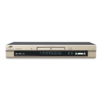
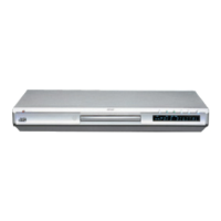
XV-S40BK/XV-S42SL/XV-S45GD
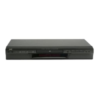
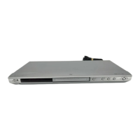
XV-S30BK/XV-E100SL
1-38
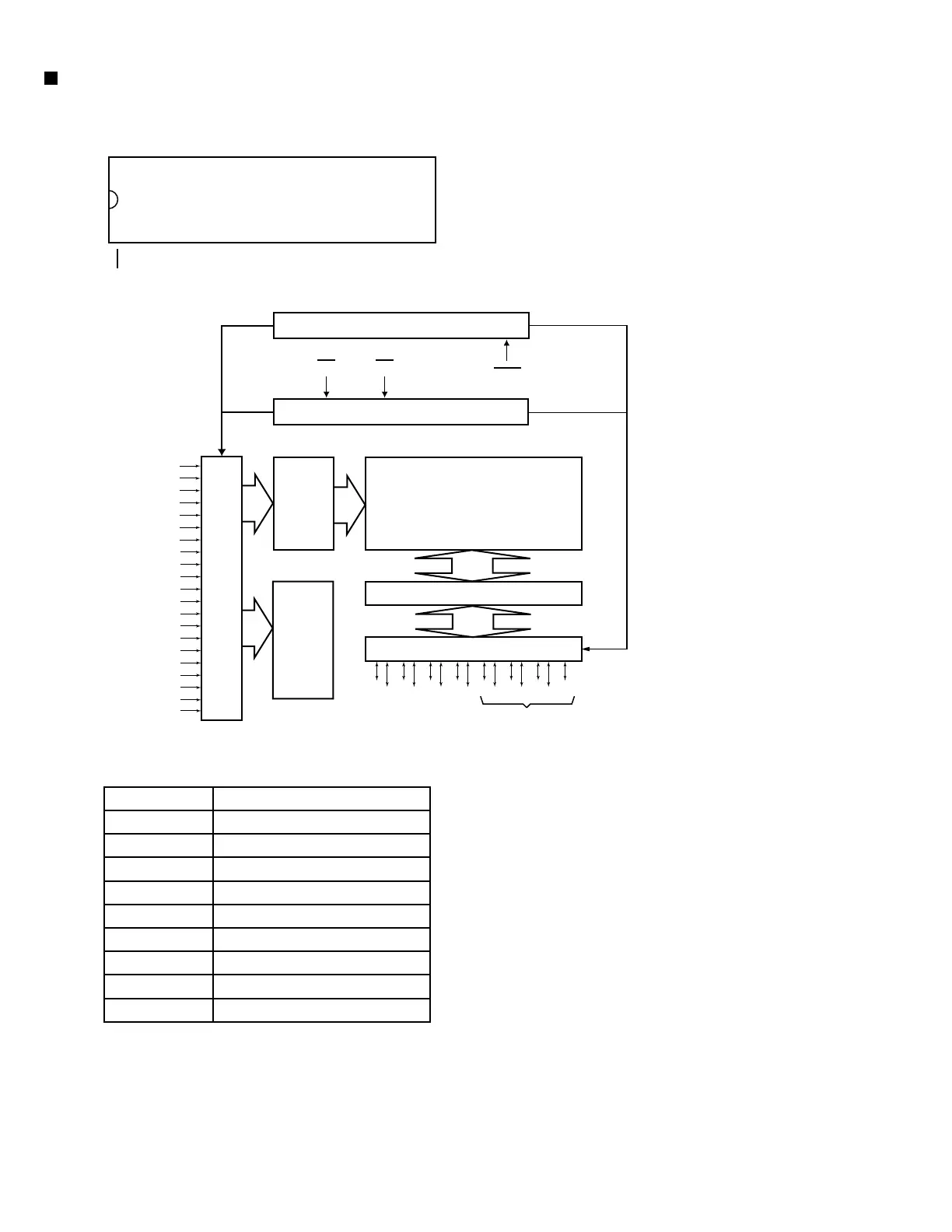
1.Pin layout
2.Block diagram
MR27V1602E1UTPX (IC402) :P2 ROM of 1,048,576word x 16 bit / 2,097,152 word x 8 bit
CE
CE
OE
OE
x 8 / x 16 Output select
BYTE
Row Decoder
Column Decoder
Memory Cell Matrix
1,048,576 x 16-Bit or 2,097,152 x 8-Bit
Multiplexer
Output Buffer
D0
D1
D14D2
D3
D4
D5
D6
D7
D8
D9
D10
D11
D12
D13
When the mode of IC outputs
eight bits, these pins are in the
state of high impedance.
Address Buffer
A0
A1
A2
A3
A4
A5
A6
A7
A8
A9
A10
A11
A12
A13
A14
A15
A16
A17
A18
A19
A20
Symbol
A0 - A20
D0 - D14
CE
OE
BYTE
Vcc
Vss
WE
WP
Function
Address Input
Data Output
Chip Enable
Output Enable
Mode Switch
Power Supply
GND
Write enable
Connect to ground
3.Pin functions
WP
A20
A9
A10
A11
A12
A13
A14
A15
A16
A17
BYTE
Vss
A0
D7
D14
D6
D13
D5
D12
D4
Vcc
1
2
3
4
5
6
7
8
9
10
11
12
13
14
15
16
17
18
19
20
21
22
44
43
42
41
40
39
38
37
36
35
34
33
32
31
30
29
28
27
26
25
24
23
WE
A19
A18
A8
A7
A6
A5
A4
A3
A2
A1
CE
Vss
OE
D0
D8
D1
D9
D2
D10
D3
D11
 Loading...