Do you have a question about the Kenwood AT-930 and is the answer not in the manual?
Details frequency range, impedance, power, dimensions, and weight of the transceiver.
Outlines transmitter power input, suppression, harmonic content, modulation, and distortion.
Details receiver circuitry, IF frequencies, sensitivity, selectivity, and stability parameters.
Provides specifications for the optional AT-930 including frequency range, impedance, and power.
Illustrates the frequency configurations for receiver and transmitter sections.
Explains the roles of VCOs, HET generation, and CAR circuits within the Signal unit.
Describes the receive signal path from antenna to the audio output stage.
Details the transmit signal path from microphone input to the final output stage.
Explains the three PLL loops used for frequency control and step generation.
Shows the block diagram of the PLL unit and its digital control interface.
Provides frequency division data for PLL control across various bands.
Details the CPU, I/O, display drivers, and memory functions of the Digital unit.
Explains the main tuning and RIT encoder operation and frequency step control.
Lists and describes the functions of various terminals on the Digital unit.
Details the block diagram, ratings, and terminal functions of the µPD8243C IC.
Lists and describes the functions of terminals on the µPD8049C-211 IC.
Explains the operation of the NB1 and NB2 noise blanker circuits.
Illustrates the noise blanker circuits (NB1, NB2) and timing charts.
Shows the speech processor block diagram and explains its function.
Describes the audio monitor circuit and the side tone generation circuit.
Explains the automatic SWR calculation and computing circuits.
Details the CW Variable Bandwidth Tuning and SSB Slope Tune operations.
Illustrates RX signal configurations and effects of CAR shifts.
Shows diagrams for CW-VBT, SSB slope-tune, and VCO bandwidth relationships.
Describes the notch filter operation and the AF-tune circuit for CW mode.
Explains the VOX, Anti-VOX circuits and their timing configuration.
Details the fan control and temperature protection circuits for final amplifiers.
Describes the timing chart for CW full break-in and send-receive switching.
Illustrates timing charts for T-R switching in various modes.
Shows the block diagram of the T-R timing control circuitry.
Provides reference data and measurement conditions for SSB and VOX circuits.
Details reference data and measurement conditions for CW full brake-in.
Explains ALC circuit, VSWR, and final overcurrent protection mechanisms.
Describes the automatic antenna tuner operation and its block diagram.
Shows the AT unit block diagram and the band data table for control.
Lists specifications for Monolithic Crystal Filters used in the Signal unit.
Details specifications for ceramic filters used in the Signal unit.
Provides specifications for optional CW and AM crystal filters.
Maximum ratings for 2SK125P transistors used in the RF unit.
Shows the block diagram for the MC145156P PLL IC in the PLL unit.
Shows the block diagram for the µPB551C PLL IC in the PLL unit.
Details the MB74LS42 IC block diagram and its function table.
Lists maximum ratings for transistors used in Digital, Signal, and Final units.
Shows the block diagram and terminal functions for the µPD8049C-211 IC.
Details the block diagram for the TC4073BP IC used in the Signal unit.
Shows the equivalent circuit and top view pinout for the MB3614 IC.
Provides the equivalent circuit and pinout for the NJM2903D IC.
Lists maximum ratings for 2SC2899 transistors and ERZ-C07DK201 diodes.
Shows equivalent circuits for UA7818UC, TA78L005AP, and HD10116 ICs.
Maximum ratings for 2SA950 transistors used in AT unit.
Details the circuit, pinout, and maximum ratings for the NJM2901 IC.
Provides the circuit and maximum ratings for the NJM2904D IC.
Shows the equivalent circuit and top view pinout for the HD10131 IC.
Details the top view pinout for the HD10125 IC.
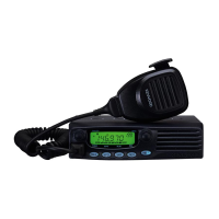
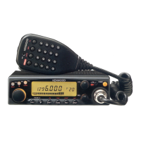
Identifies controls, knobs, and jacks on the front panel of the transceiver.
Details connectors, jacks, and features on the rear panel.
Shows the component placement on the Low Pass Filter (LPF) unit PCB.
Lists transistors and diodes used on the LPF unit board.
Illustrates component placement on the Switch unit PCB.
Lists transistors, diodes, and capacitors used on the Switch unit.
Shows component placement on the Switch unit PCB (continued).
Lists transistors, diodes, and ICs used on the Switch unit.
Illustrates component placement on the Power Supply unit PCB.
Shows component placement on the RF unit PCB.
Lists transistors and diodes used on these PCBs.
Shows component placement on the Power Supply unit PCB (continued).
Illustrates component placement on the RF unit PCB (continued).
Lists transistors, diodes, and ICs used on these PCBs.
Shows component placement on the PLL unit PCB.
Lists transistors, ICs, and capacitors used on the PLL unit.
Presents the detailed circuit schematic for the PLL unit.
Shows component placement on the Digital unit PCB.
Lists transistors, ICs, and capacitors used on the Digital unit.
Provides the circuit schematic for the Digital unit.
Shows circuit schematics for the Main and RIT Encoder units.
Illustrates component placement on the AT unit PCB.
Lists variable capacitors, motors, and transistors used on the AT unit.
Presents the detailed circuit schematic for the AT unit.
Shows component placement on the 100W Final unit PCB.
Illustrates component placement on Main and RIT Encoder unit PCBs.
Lists transistors and ICs used on these PCBs.
Shows component placement on the Signal unit PCB (part A/2).
Lists transistors, ICs, and capacitors used on the Signal unit PCB.
Illustrates component placement on the Signal unit PCB (part B/2).
Lists transistors, ICs, and capacitors used on the Signal unit PCB.
Shows the foil side component layout for the Signal unit PCB (part A/2).
Lists transistors, ICs, and diodes used on the Signal unit PCB.
Provides instructions and cautions for soldering chip capacitors.
Lists diodes, varistors, and zener diodes with part numbers and references.
Lists LEDs, FETs, and transistors with part numbers and references.
Lists various integrated circuits (ICs) with part numbers and references.
Details capacitors used in the Digital unit with part numbers and references.
Maps transistors, FETs, and ICs to their terminal addresses and locations.
Lists various capacitors, connectors, and coils with part numbers.
Lists resistors, inline blocks, relays, and jumpers with part numbers.
Lists capacitors, connectors, and trimmers for the PLL unit.
Lists capacitors, ICs, and transistors used in the Digital unit.
Lists trimmers, capacitors, and connectors for the RF unit.
Lists coils, resistors, relays, and motors for the RF unit.
Lists trimmers, capacitors, coils, resistors, relays, and motors for the Switch unit.
Details various capacitors used in the Signal unit with part numbers.
Lists capacitors, connectors, and trimmers used in the PLL unit.
Lists capacitors, connectors, and coils for the Digital unit.
Lists trim pots, resistors, relays, and jumpers for the Digital unit.
Lists capacitors, trimmers, and coils for Main and RIT Encoder units.
Lists capacitors, coils, and resistors for the 100W Final unit.
Details various capacitors used in the Signal unit with part numbers.
Lists capacitors, connectors, and trimmers for the PLL unit.
Lists capacitors, connectors, and coils with part numbers.
Lists trim pots, resistors, relays, and jumpers with part numbers.
Details packing materials and the procedure for packaging the transceiver.
Lists capacitors, ICs, and transistors used in the Digital unit.
Lists trimmers, capacitors, and connectors for the RF unit.
Lists coils, resistors, relays, and motors for the RF unit.
Lists trimmers, capacitors, coils, resistors, relays, and motors for the Switch unit.
Lists capacitors, connectors, and coils with part numbers.
Lists trim pots, resistors, relays, and jumpers with part numbers.
Details packing materials and the procedure for packaging the transceiver.
Instructions for removing the front panel and servicing its components.
Cautions regarding disassembly of the rear panel and its terminals.
General cautions for disassembling internal components like transformers and PC boards.
Specific cautions for rear panel and transformer removal.
Steps for removing PC boards and electrolytic capacitors.
Instructions for removing display tubes, knobs, and band switch assemblies.
Detailed steps for removing front panel knobs, seals, and switch units.
Detailed cautions for rear panel and internal component disassembly.
Lists necessary test equipment for performing adjustments.
Specifies initial settings for front and rear panel controls before adjustments.
Details adjustments for power supply, TX control, SWR, and VCO levels.
Covers adjustments for the standard oscillator, multiplier, and VCOs.
Details adjustments for PLL-BPF, PLL, VCO-BPF, HET, and VCO level.
Covers duty ratio and phase difference adjustments for Main encoder.
Details duty ratio and phase difference adjustments for the RIT encoder.
Describes the adjustment procedure for the CAR-1 signal in receive mode.
Covers adjustments for CAR-2, CAR-3, CW Pitch, 355kHz BPF, and 0.1-30MHz BPF.
Details adjustments for 44.93MHz MCF and SSB Slope Tune functions.
Covers adjustments for the RX IF amplifier and Notch filter.
Describes the adjustment procedure for the TX band pass filters.
Covers adjustments for TX drive, IF amplifier, and meter points.
Details adjustments for the 100W final stage bias and current limiter.
Covers power output adjustments for CW, AM, and TUNE modes.
Details adjustments for protection circuits, SWR meter, and Vc meter.
Describes how to adjust the SSB mode frequency response.
Covers carrier suppression adjustments and ALC meter calibration.
Details adjustments for the speech processor and monitor level.
Covers adjustments for audio mix balance and side tone pitch.
Describes the procedure for tuning the automatic antenna tuner.
Covers transceiver reset and checks for band switching operation.
Details checks for dial step operation, RIT, and memory write functions.
Covers checks for memory recall and the A=B function.
Details checks for microphone UP/DOWN controls and D.LOCK function.
Diagram showing adjustment points on Power Supply, Final, PLL, AT, and Encoder units.
Diagram showing adjustment points on RF, Signal, and Main Encoder units.
Shows signal levels throughout the receiver section.
Illustrates signal levels throughout the transmitter section.
Detailed RX signal path with voltage levels at various points.
Detailed TX signal path with voltage levels at various points.
Shows the overall block diagram of the transceiver, illustrating major units and signal flow.
Details the SP-930 speaker's size, input, impedance, and frequency response.
Lists parts for the SP-930 and refers to its schematic diagram.
Provides step-by-step instructions for disassembling the SP-930 unit.
Illustrates the packing procedure and lists the materials required for shipping.
Details the AT-930 antenna tuner's frequency range, impedance, and power handling.
Lists parts for the AT-930 and provides disassembly instructions.
Provides specifications and parts list for the SO-1 unit.
Details the frequency counter adjustment procedure for the SO-1 unit.
Describes common through-plated hole defects in the Digital unit and their symptoms.
Lists specific symptoms related to through-hole defects in the Digital unit.
Lists specific symptoms related to through-hole defects in the Digital unit.
Shows numbered component locations on the Digital unit PCB.
| Brand | Kenwood |
|---|---|
| Model | AT-930 |
| Category | Transceiver |
| Language | English |